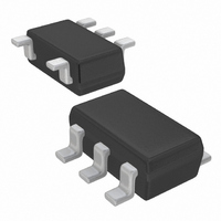
XC6222B281MR-G Torex Semiconductor Ltd, XC6222B281MR-G Datasheet - Page 9

XC6222B281MR-G
Manufacturer Part Number
XC6222B281MR-G
Description
IC REG LDO 2.8V SOT-25
Manufacturer
Torex Semiconductor Ltd
Datasheet
1.XC6222B28BMR-G.pdf
(26 pages)
Specifications of XC6222B281MR-G
Regulator Topology
Positive Fixed
Voltage - Output
2.8V
Voltage - Input
Up to 6V
Voltage - Dropout (typical)
0.16V @ 300mA
Number Of Regulators
1
Current - Output
700mA (Min)
Current - Limit (min)
720mA
Operating Temperature
-40°C ~ 85°C
Mounting Type
Surface Mount
Package / Case
SOT-23-5, SC-74A, SOT-25
Lead Free Status / RoHS Status
Lead free / RoHS Compliant
Other names
893-1141-2
The entire XC6222 circuitry can be turned off via the CE pin signal. In shutdown mode, output at the V
For the XC6222A/B series, the output voltage becomes unstable, when the CE pin is left open. If this CE pin voltage is set with
<Current Limiter, Short-Circuit Protection>
The XC6222 series’ fold-back circuit operates as an output current limiter and a short protection circuit for the output pin.
When the load current reaches the current limit level, the fixed current limiter circuit operates and output voltage drops. When
the output pin is short-circuited to the V
<Thermal Shutdown>
When the junction temperature of the built-in driver transistor reaches the temperature limit level (150℃ TYP.), the thermal
shutdown circuit operates and the driver transistor will be turned OFF. The IC resumes its operation when the thermal
shutdown function is released and the IC’s operation is automatically restored because the junction temperature drops to the
level of 125℃ (TYP.) as the thermal shutdown release voltage.
■OPERATIONAL EXPLANATION (Continued)
<C
<CE Pin>
down to the V
R1 and R2 while the power supply is applied to the V
the specified voltage range, the logic is fixed and the IC will operate normally. However, the supply current may increase as a
result of shoot-through current in the IC's internal circuitry when a medium voltage is input to the CE pin. With the XC6222C/D
series, when the CE pin is left open, output voltage is fixed to V
■NOTES ON USE
XC6222B/D series can discharge the electric charge stored in the output capacitor (C
enables the whole IC circuit to be turned off, is inputted via the N-channel transistor located between the V
pin (cf. BLOCK DIAGRAM). The CL auto-discharge resistance value is set at 530Ω(TYP.). The discharge time of the output
capacitor (C
C
discharge via the N-channel transistor is calculated by the following formula.
2. Where wiring impedance is high, operations may become unstable due to noise and/or phase lag depending on
1
L
.
L
where
auto-discharge resistance value [R
output current.
Please use this IC within the stated absolute maximum ratings. The IC is liable to malfunction should the ratings be
exceeded.
Auto-Discharge Function>
Please wire the input capacitor (C
V: Output voltage after discharge
V
τ: C
OUT (E)
t: Discharge time
V = V
L
auto-discharge resistance R
L
OUT(E)
) is set by the CL auto-discharge resistance (R) and the output capacitor (C
: Output voltage
SS
level via R1 & R2. However, with the XC6222B series, the C
x e
–t/ τ
, or t=
τ
IN
In ( V / V
DCHG
SS
) and the output capacitor (C
DCHG
pin, the current is decreased to a level of 55mA.
] and the output capacitor value (C
×Output capacitor (C
OUT(E)
IN
)
pin. Therefore, time until the V
SS
level.
L
) value C)
L
) as close to the IC as possible.
L
auto-discharge resistor is connected in parallel to
L
) as τ(τ=C x R
L
), when a low signal to the CE pin, which
OUT
L
). By setting the time constant of the
pin reaches the V
DCHG
), the output voltage after
OUT
OUT
SS
pin will be pulled
pin and the V
level is shorter.
XC6222
Series
9/26
SS


