LD1117ADT12TR STMicroelectronics, LD1117ADT12TR Datasheet - Page 14
LD1117ADT12TR
Manufacturer Part Number
LD1117ADT12TR
Description
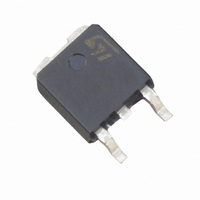
IC REG LDO POS 1A 1.2V D-PAK
Manufacturer
STMicroelectronics
Specifications of LD1117ADT12TR
Regulator Topology
Positive Fixed
Voltage - Output
1.2V
Voltage - Input
Up to 15V
Voltage - Dropout (typical)
1.15V @ 1A
Number Of Regulators
1
Current - Output
1.2A
Operating Temperature
0°C ~ 125°C
Mounting Type
Surface Mount
Package / Case
TO-252-2, DPak (2 Leads + Tab), TO-252AA, SC-63
Number Of Outputs
1
Polarity
Positive
Input Voltage Max
10 V
Output Voltage
1.2 V
Output Type
Fixed
Dropout Voltage (max)
1.1 V at 100 mA
Output Current
1000 mA
Line Regulation
6 mV / V
Load Regulation
10 mV
Voltage Regulation Accuracy
2 %
Maximum Power Dissipation
12 W
Maximum Operating Temperature
+ 125 C
Mounting Style
SMD/SMT
Minimum Operating Temperature
0 C
Lead Free Status / RoHS Status
Lead free / RoHS Compliant
Current - Limit (min)
-
Lead Free Status / Rohs Status
Lead free / RoHS Compliant
Other names
497-6011-2
Available stocks
Company
Part Number
Manufacturer
Quantity
Price
Company:

Part Number:
LD1117ADT12TR
Manufacturer:
ST
Quantity:
15 000
Part Number:
LD1117ADT12TR
Manufacturer:
ST
Quantity:
20 000


LD1117A adjustable: application note LD1117AXX12, LD1117AXX18, LD1117AXX33, LD1117AXX
7
Figure 10. Adjustable output voltage application
Figure 11. Adjustable output voltage application with improved ripple rejection
14/24
LD1117A adjustable: application note
The LD1117A adjustable has a thermal stabilized 1.25 ± 0.012 V reference voltage between
the OUT and ADJ pins. I
R
V
In normal application R
be considered in the V
V
In order to have the better load regulation it is important to realize a good Kelvin connection
of R
ADJ pin, while R
Load pin. Ripple rejection can be improved by introducing a 10 µF electrolytic capacitor
placed in parallel to the R
OUT
OUT
1
is normally fixed to 120 Ω. From
1
= V
= V
and R
REF
REF
2
+ R
resistors. In particular R
(1 + R
2
2
ground connection must be placed as near as possible to the negative
(I
2
ADJ
/ R
OUT
2
+I
1
ADJ
value is in the range of few kΩ, so the R
).
2
R1
calculation; then the above expression becomes:
resistor (see
) = V
is 60 µA typ. (120 µA max.) and ΔI
Doc ID 7194 Rev 23
REF
Figure 7
+ R
1
connection must be realized very close to OUT and
Figure
2
(I
ADJ
we obtain:
10).
+V
REF
/R
1
) = V
ADJ
REF
2
x I
is 1 µA typ. (5 µA max.).
(1 + R
ADJ
product could not
2
/ R
1
) + R
2
x I
ADJ
.
Related parts for LD1117ADT12TR
Image
Part Number
Description
Manufacturer
Datasheet
Request
R

Part Number:
Description:
STMicroelectronics [RIPPLE-CARRY BINARY COUNTER/DIVIDERS]
Manufacturer:
STMicroelectronics
Datasheet:
Part Number:
Description:
STMicroelectronics [LIQUID-CRYSTAL DISPLAY DRIVERS]
Manufacturer:
STMicroelectronics
Datasheet:

Part Number:
Description:
BOARD EVAL FOR MEMS SENSORS
Manufacturer:
STMicroelectronics
Datasheet:
Part Number:
Description:
NPN TRANSISTOR POWER MODULE
Manufacturer:
STMicroelectronics
Datasheet:
Part Number:
Description:
TURBOSWITCH ULTRA-FAST HIGH VOLTAGE DIODE
Manufacturer:
STMicroelectronics
Datasheet:
Part Number:
Description:
Manufacturer:
STMicroelectronics
Datasheet:
Part Number:
Description:
DIODE / SCR MODULE
Manufacturer:
STMicroelectronics
Datasheet:
Part Number:
Description:
DIODE / SCR MODULE
Manufacturer:
STMicroelectronics
Datasheet:
Part Number:
Description:
Search -----> STE16N100
Manufacturer:
STMicroelectronics
Datasheet:
Part Number:
Description:
Search ---> STE53NA50
Manufacturer:
STMicroelectronics
Datasheet:
Part Number:
Description:
NPN Transistor Power Module
Manufacturer:
STMicroelectronics
Datasheet: