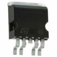
LD1580P2T-R STMicroelectronics, LD1580P2T-R Datasheet

LD1580P2T-R
Specifications of LD1580P2T-R
LD1580P2T-R
Available stocks
Related parts for LD1580P2T-R
LD1580P2T-R Summary of contents
Page 1
... April 2008 power dissipation in case of insufficient heatsinking. On chip trimming allows the regulator to reach a very tight output voltage tolerance, within ± the maximum output current and over the full temperature range. Order code LD1580P2T-R Rev 5 LD1580XX ² P PAK Packaging tape and reel 1/15 www ...
Page 2
Contents 1 Diagram . . . . . . . . . . . . . . . . . . . . . . . . . . . . . . . . . . . . . ...
Page 3
Diagram Figure 1. Schematic diagram 3/15 ...
Page 4
Pin configuration Figure 2. Pin connections (top view) 4/15 ...
Page 5
Maximum ratings Table 2. Absolute maximum ratings Symbol POWER POWER CONTROL CONTROL I Output current OUT P Power dissipation D T Storage temperature range STG T Operating junction temperature range OP Note: Absolute ...
Page 6
Typical application Figure 3. Typical application circuits 6/15 R ⎛ ⎞ 2 ⋅ ------ - ⎝ ⎠ O REF R 1 ...
Page 7
Electrical characteristics Table 4. Electrical characteristics for LD1580 ( 100 µF, unless otherwise specified) OUT Symbol Parameter V Output voltage O ΔV Line regulation O ΔV Load regulation pin current C CONTROL I Adjust ...
Page 8
Typical characteristics (unless otherwise specified T Figure 4. Output voltage vs temperature Figure 6. Minimum V POWER current Figure 8. V pin current vs temp. CONTROL 8/ ° 330 µ Figure 5. ...
Page 9
Figure 10. V pin current vs output CONTROL current Figure 12. Quiescent current vs temperature Figure 14. Line transient response V =3.3V 7V, I POWER CONTROL OUT Figure 11. Output current limit vs temperature Figure 13. Supply ...
Page 10
Figure 16. Load transient response V =V =5V POWER CONTROL Figure 18. Load transient response V =V =5V POWER CONTROL 10/15 Figure 17. Load transient response V =V =5V POWER CONTROL ...
Page 11
Package mechanical data In order to meet environmental requirements, ST offers these devices in ECOPACK packages. These packages have a lead-free second level interconnect. The category of second Level Interconnect is marked on the package and on the inner ...
Page 12
Dim. Min. A 4.30 A1 2.40 A2 0.03 b 0.80 c 0.45 c2 1. 10. 3.20 e1 6.60 L 13.70 L2 1.25 L3 0. 0° 12/ PAK mechanical ...
Page 13
Tape & reel D PAK-P mm. Dim. Min. Typ 12.8 13 10.50 10.6 Bo 15.70 15.80 Ko 4.80 4.90 Po 3.9 4.0 P 11.9 12 PAK-D PAK/A-P PAK/A ...
Page 14
Revision history Table 5. Document revision history Date Revision 08-Sep-2005 3 09-May-2007 4 16-Apr-2008 5 14/15 Changes Order codes updated. Order codes updated. Modified: Table 1 on page 1. ...
Page 15
... Information in this document is provided solely in connection with ST products. STMicroelectronics NV and its subsidiaries (“ST”) reserve the right to make changes, corrections, modifications or improvements, to this document, and the products and services described herein at any time, without notice. All ST products are sold pursuant to ST’s terms and conditions of sale. ...


