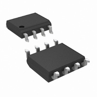
LP2951ACM/NOPB National Semiconductor, LP2951ACM/NOPB Datasheet - Page 5

LP2951ACM/NOPB
Manufacturer Part Number
LP2951ACM/NOPB
Description
IC VREG ADJ MICRPWR 8-SOIC
Manufacturer
National Semiconductor
Type
Voltage Regulatorr
Specifications of LP2951ACM/NOPB
Regulator Topology
Positive Adjustable
Voltage - Output
1.24 ~ 29 V
Voltage - Input
Up to 30V
Voltage - Dropout (typical)
0.38V @ 100mA
Number Of Regulators
1
Current - Output
100mA
Operating Temperature
-40°C ~ 125°C
Mounting Type
Surface Mount
Package / Case
8-SOIC (3.9mm Width)
Current, Input Bias
20 nA
Current, Output
100 mA
Current, Supply
75 μA
Package Type
SOP
Regulation, Line
0.03 %
Regulation, Load
0.04 %
Regulator Type
Low Dropout
Temperature, Operating, Range
-40 to +125 °C
Voltage, Dropout
380 mV
Voltage, Input
30 V
Voltage, Noise
430 μV
Voltage, Output
5 V
Number Of Outputs
1
Polarity
Positive
Input Voltage Max
30 V
Output Voltage
1.24 V to 29 V
Output Type
Adjustable
Dropout Voltage (max)
0.08 V at 100 uA
Output Current
0.1 A
Line Regulation
0.1 %
Load Regulation
0.1 %
Voltage Regulation Accuracy
+/- 0.5 %
Maximum Operating Temperature
+ 125 C
Mounting Style
SMD/SMT
Minimum Operating Temperature
- 40 C
Reference Voltage
1.25 V
Lead Free Status / RoHS Status
Lead free / RoHS Compliant
Current - Limit (min)
-
Lead Free Status / Rohs Status
RoHS Compliant part
Electrostatic Device
Other names
*LP2951ACM
*LP2951ACM/NOPB
LP2951ACM
*LP2951ACM/NOPB
LP2951ACM
Available stocks
Company
Part Number
Manufacturer
Quantity
Price
Company:
Part Number:
LP2951ACM/NOPB
Manufacturer:
AD
Quantity:
1 982
All Voltage Options
Temperature
Coefficient
Feedback Pin Bias
Current Temperature
Coefficient
Error Comparator
Output Leakage
Current
Output Low
Voltage
Upper Threshold
Voltage
Lower Threshold
Voltage
Hysteresis
Shutdown Input
Input
Logic
Voltage
Shutdown Pin Input
Current
Regulator Output
Current in Shutdown
Electrical Characteristics
Note 1: Absolute Maximum Ratings are limits beyond which damage to the device may occur. Operating Ratings are conditions under which operation of the device
is guaranteed. Operating Ratings do not imply guaranteed performance limits. For guaranteed performance limits and associated test conditions, see the Electrical
Characteristics tables.
Note 2: Unless otherwise specified all limits guaranteed for V
appearing in boldface type apply over the entire junction temperature range for operation. Limits appearing in normal type apply for T
conditions for the 8-pin versions are FEEDBACK tied to V
Note 3: Guaranteed and 100% production tested.
Note 4: Guaranteed but not 100% production tested. These limits are not used to calculate outgoing AQL levels.
Note 5: Dropout Voltage is defined as the input to output differential at which the output voltage drops 100 mV below its nominal value measured at 1V differential.
At very low values of programmed output voltage, the minimum input supply voltage of 2V (2.3V over temperature) must be taken into account.
Note 6: Comparator thresholds are expressed in terms of a voltage differential at the Feedback terminal below the nominal reference voltage measured at V
(V
programmed output voltage of 5V, the Error output is guaranteed to go low when the output drops by 95mV x 5V/1.235V = 384 mV. Thresholds remain constant as
a percent of V
Note 7: V
Note 8: The junction-to-ambient thermal resistances are as follows: 180˚C/W and 160˚C/W for the TO-92 package with 0.40 inch and 0.25 inch leads to the printed
circuit board (PCB) respectively, 105˚C/W for the molded plastic DIP (N), 130˚C/W for the ceramic DIP (J), 160˚C/W for the molded plastic SOP (M), 200˚C/W for
the molded plastic MSOP (MM), and 160˚C/W for the metal can package (H). The above thermal resistances for the N, J, M, and MM packages apply when the
package is soldered directly to the PCB. Junction-to-case thermal resistance for the H package is 20˚C/W. Junction-to-case thermal resistance for the TO-252
package is 5.4˚C/W. The value of θ
thermal vias. For details of thermal resistance and power dissipation for the LLP package, refer to Application Note AN-1187.
Note 9: May exceed input supply voltage.
O
NOM + 1)V. To express these thresholds in terms of output voltage change, multiply by the error amplifier gain = V
Parameter
ref
≤ V
out
out
as V
≤ (V
out
in
is varied, with the dropout warning occurring at typically 5% below nominal, 7.5% guaranteed.
− 1V), 2.3V ≤ V
V
V
0.5)V
I
(Note 6)
(Note 6)
(Note 6)
Low (Regulator
ON)
High (Regulator
OFF)
V
V
(Note 11)
OL
OH
in
shutdown
shutdown
= (V
= 400µA
Conditions
= 30V
JA
(Note 2)
for the LLP package is typically 51˚C/W but is dependent on the PCB trace area, trace material, and the number of layers and
O
NOM −
= 2.4V
= 30V
in
≤ 30V, 100µA ≤ I
(Note 2) (Continued)
0.01
Typ
150
450
0.1
1.3
60
75
15
30
3
TAP
IN
L
, OUTPUT tied to SENSE, and V
LP2951
≤ 100mA, T
= (V
(Notes 3, 16)
ONOM
Tested
Limit
250
400
140
100
600
750
0.6
2.0
40
25
95
50
10
20
1
2
+ 1)V, I
J
≤ T
JMAX
L
7
= 100µA and C
0.01
Typ
150
450
0.1
1.3
60
75
15
30
.
3
LP2950AC-XX
LP2951AC-XX
(Note 3) (Note 4)
Tested
Limit
250
600
SHUTDOWN
40
95
50
10
1
L
= 1µF for 5V versions and 2.2µF for 3V and 3.3V versions. Limits
Design
≤ 0.8V.
Limit
400
140
100
750
0.7
2.0
25
20
2
0.01
Typ
150
450
0.1
1.3
60
75
15
30
out
3
/V
ref
LP2950C-XX
LP2951C-XX
(Note 3) (Note 4)
= (R1 + R2)/R2.For example, at a
Tested
Limit
250
600
40
95
50
10
1
A
= T
Design
J
Limit
400
140
100
750
0.7
2.0
= 25˚C. Additional
25
20
2
mV max
mV max
mV max
mV max
µA max
µA max
mV min
mV min
µA max
µA max
µA max
µA max
µA max
µA max
V max
V min
Units
nA/˚C
mV
V
in
=


