LP38512TJ-1.8/NOPB National Semiconductor, LP38512TJ-1.8/NOPB Datasheet - Page 11
LP38512TJ-1.8/NOPB
Manufacturer Part Number
LP38512TJ-1.8/NOPB
Description
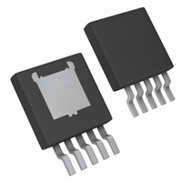
IC REG LDO 1.5A 1.8V TO263-5
Manufacturer
National Semiconductor
Datasheet
1.LP38512TS-1.8EV.pdf
(14 pages)
Specifications of LP38512TJ-1.8/NOPB
Regulator Topology
Positive Fixed
Voltage - Output
1.8V
Voltage - Input
2.25 ~ 5.5 V
Voltage - Dropout (typical)
0.25V @ 1.5A
Number Of Regulators
1
Current - Output
1.5A (Max)
Operating Temperature
-40°C ~ 125°C
Mounting Type
Surface Mount
Package / Case
TO-263-5 Thin
Lead Free Status / RoHS Status
Lead free / RoHS Compliant
Current - Limit (min)
-
Other names
LP38512TJ-1.8TR
Available stocks
Company
Part Number
Manufacturer
Quantity
Price
Company:

Part Number:
LP38512TJ-1.8/NOPB
Manufacturer:
National Semiconductor
Quantity:
1 975


POWER DISSIPATION/HEATSINKING
A heatsink may be required depending on the maximum pow-
er dissipation (P
(T
of the package. Under all possible conditions, the junction
temperature (T
Operating Ratings. The total power dissipation of the device
is given by:
where I
(specified under Electrical Characteristics).
The maximum allowable junction temperature rise (ΔT
pends on the maximum expected ambient temperature (T
(MAX)
temperature (T
The maximum allowable value for junction to ambient Ther-
mal Resistance, θ
HEATSINKING TO-263 PACKAGE
The TO-263 and the TO-263 THIN packages use the copper
plane on the PCB as a heatsink. The tab, or DAP, of these
packages are soldered to the copper plane for heat sinking.
Figure 3 shows a curve for the θ
different copper area sizes, using a typical PCB with 1 ounce
copper and no solder mask over the copper area for heat
sinking.
A(MAX)
) of the application, and the maximum allowable junction
) of the application, and the thermal resistance (θ
P
GND
D
= ( (V
is the operating ground current of the device
J(MAX)
J
ΔT
) must be within the range specified in the
IN
θ
JA
D(MAX)
−V
J
JA
, can be calculated using the formula:
):
= T
OUT
= ΔT
J(MAX)
), maximum ambient temperature
) x I
J
/ P
OUT
− T
D(MAX)
) + (V
A(MAX)
JA
of TO-263 package for
FIGURE 2. ERROR Flag Operation, biased from V
IN
x I
GND
)
J
) de-
(1)
(2)
(3)
JA
A
)
11
As shown in the figure, increasing the copper area beyond 1
square inch produces very little improvement. The minimum
value for θ
PCB is 32°C/W.
Figure 4 shows the maximum allowable power dissipation for
TO-263 packages for different ambient temperatures, assum-
ing θ
125°C.
FIGURE 3. θ
FIGURE 4. Maximum Power Dissipation vs Ambient
JA
is 35°C/W and the maximum junction temperature is
JA
Temperature for TO-263 Package
for the TO-263 package mounted to a two-layer
JA
vs Copper (1 Ounce) Area for TO-263
IN
package
20183035
20183034
20183036
www.national.com
Related parts for LP38512TJ-1.8/NOPB
Image
Part Number
Description
Manufacturer
Datasheet
Request
R

Part Number:
Description:
IC REG LDO 1.5A ADJ TO263-5
Manufacturer:
National Semiconductor
Datasheet:

Part Number:
Description:
1.5a Fast-transient Response Adjustable Low-dropout Linear Voltage Regulator
Manufacturer:
National Semiconductor Corporation
Datasheet:

Part Number:
Description:
National Semiconductor [8-Bit D/A Converter]
Manufacturer:
National Semiconductor
Datasheet:
Part Number:
Description:
National Semiconductor [Media Coprocessor]
Manufacturer:
National Semiconductor
Datasheet:
Part Number:
Description:
Digitally Controlled Tone and Volume Circuit with Stereo Audio Power Amplifier, Microphone Preamp Stage and National 3D Sound
Manufacturer:
National Semiconductor
Datasheet:
Part Number:
Description:
Digitally Controlled Tone and Volume Circuit with Stereo Audio Power Amplifier, Microphone Preamp Stage and National 3D Sound
Manufacturer:
National Semiconductor
Datasheet:
Part Number:
Description:
AC97 Rev 2 Codec with Sample Rate Conversion and National 3D Sound
Manufacturer:
National Semiconductor
Part Number:
Description:
Manufacturer:
National Semiconductor
Datasheet:
Part Number:
Description:
Manufacturer:
National Semiconductor
Datasheet:
Part Number:
Description:
General Purpose, Low Voltage, Low Power, Rail-to-Rail Output Operational Amplifiers
Manufacturer:
National Semiconductor
Datasheet:
Part Number:
Description:
8-bit 20 MSPS flash A/D converter.
Manufacturer:
National Semiconductor
Datasheet:
Part Number:
Description:
Low Noise Quad Operational Amplifier
Manufacturer:
National Semiconductor
Datasheet:
Part Number:
Description:
Quad Differential Line Receivers
Manufacturer:
National Semiconductor
Datasheet:
Part Number:
Description:
Quad High Speed Trapezoidal? Bus Transceiver
Manufacturer:
National Semiconductor
Datasheet: