LM2940S-12/NOPB National Semiconductor, LM2940S-12/NOPB Datasheet - Page 6
LM2940S-12/NOPB
Manufacturer Part Number
LM2940S-12/NOPB
Description
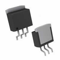
IC REGULATOR LDO 1A TO-263
Manufacturer
National Semiconductor
Datasheet
1.LM2940IMP-5.0NOPB.pdf
(20 pages)
Specifications of LM2940S-12/NOPB
Regulator Topology
Positive Fixed
Voltage - Output
12V
Voltage - Input
13.6 ~ 26 V
Voltage - Dropout (typical)
0.5V @ 1A
Number Of Regulators
1
Current - Output
1A
Operating Temperature
-40°C ~ 125°C
Mounting Type
Surface Mount
Package / Case
TO-263-3, D²Pak (3 leads + Tab), TO-263AA
Number Of Outputs
1
Polarity
Positive
Input Voltage Max
26 V
Output Voltage
12 V
Output Type
Fixed
Dropout Voltage (max)
0.8 V At 1 A
Output Current
1 A (Typ)
Line Regulation
120 mV
Load Regulation
120 mV
Maximum Operating Temperature
+ 125 C
Mounting Style
SMD/SMT
Minimum Operating Temperature
- 40 C
Voltage Regulator Type
Linear
Topology
LDO
Regulator Output Type
Fixed
Polarity Type
Positive
Input Voltage (min)
13.6V
Input Voltage (max)
26V
Package Type
TO-263
Operating Temp Range
-40C to 125C
Operating Temperature Classification
Automotive
Dropout Voltage@current (typ)
0.5@1A/0.11@100mA
Pin Count
3 +Tab
Mounting
Surface Mount
Quiescent Current (max)
15mA
Lead Free Status / RoHS Status
Lead free / RoHS Compliant
Current - Limit (min)
-
Lead Free Status / Rohs Status
Details
Other names
*LM2940S-12
*LM2940S-12/NOPB
LM2940S-12
*LM2940S-12/NOPB
LM2940S-12


www.national.com
Ripple Rejection
Long Term
Stability
Dropout Voltage
Short Circuit
Current
Maximum Line
Transient
Reverse Polarity
DC Input
Voltage
Reverse Polarity
Transient Input
Voltage
Thermal Resistance
Junction-to-Case, θ
Thermal Resistance
Junction-to-Ambient, θ
Thermal Performance
Note 1: Absolute Maximum Ratings are limits beyond which damage to the device may occur. Operating Conditions are conditions under which the device
functions but the specifications might not be guaranteed. For guaranteed specifications and test conditions see the Electrical Characteristics.
Note 2: The maximum allowable power dissipation is a function of the maximum junction temperature, T
the ambient temperature, T
shutdown. The value of θ
SOT-223 package. The effective value of θ
θ
and power dissipation for the LLP package, refer to Application Note AN-1187. It is recommended that 6 vias be placed under the center pad to improve thermal
performance.
Note 3: Refer to JEDEC J-STD-020C for surface mount device (SMD) package reflow profiles and conditions. Unless otherwise stated, the temperature and time
are for Sn-Pb (STD) only.
Note 4: ESD rating is based on the human body model, 100 pF discharged through 1.5 kΩ.
Note 5: All limits are guaranteed at T
All limits at T
methods.
Note 6: All limits are guaranteed at T
All limits are 100% production tested and are used to calculate Outgoing Quality Levels.
Note 7: Output current will decrease with increasing temperature but will not drop below 1A at the maximum specified temperature.
JA
Parameter
for the LLP package is specifically dependent on PCB trace area, trace material, and the number of layers and thermal vias. For improved thermal resistance
A
Output Voltage (V
= T
J
= 25°C are 100% production tested. All limits at temperature extremes are guaranteed via correlation using standard Statistical Quality Control
(JC)
f
I
LM2940
LM2940C
f
I
I
I
(Note 7)
R
LM2940, T
LM2940/883, T
LM2940C, T
R
LM2940, LM2940/883
LM2940C
R
LM2940, T
LM2940/883, T
LM2940C, T
O
O
O
O
O
O
O
O
O
(JA)
JA
= 120 Hz, 1 V
= 100 mA
= 1 kHz, 1 V
= 5 mA
= 1A
= 100 mA
A
= 100Ω
= 100Ω
= 100Ω
(for devices in still air with no heatsink) is 60°C/W for the TO-220 package, 80°C/W for the TO-263 package, and 174°C/W for the
. Exceeding the maximum allowable power dissipation will cause excessive die temperature, and the regulator will go into thermal
Conditions
A
A
≤
≤
O
= T
= T
)
≤
≤
100 ms
100 ms
3-Lead TO-220
3-Lead TO-263
3-Lead TO-220 (Note 2)
3-Lead TO-263 (Note 2)
SOT-223(Note 2)
8-Lead LLP (Note 2)
J
J
rms
1 ms
1 ms
= 25°C only (standard typeface) or over the entire operating temperature range of the indicated device (boldface type).
= 25°C only (standard typeface) or over the entire operating temperature range of the indicated device (boldface type).
≤
≤
JA
rms
,
20 ms
20 ms
can be reduced by using a heatsink (see Application Hints for specific information on heatsinking). The value of
,
Typ
110
−30
−30
−75
−55
0.5
1.9
66
66
48
75
55
LM2940
(Note 5)
150/200
−15/−15
−50/−50
−45/−45
0.8/1.0
54/48
60/60
Limit
−15
1.6
54
45
12V
6
LM2940/833
−15/−15
−45/−45
(Note 6)
150/200
0.7/1.0
1.6/1.3
52/46
40/40
Limit
174
J
60
80
35
, the junction-to-ambient thermal resistance, θ
4
4
Typ
110
−30
−55
0.5
1.9
64
60
55
LM2940
−45/−45
(Note 5)
150/200
0.8/1.0
Limit
−15
1.6
52
45
15V
LM2940/833
(Note 6)
150/200
−15/−15
−45/−45
0.7/1.0
1.6/1.3
48/42
40/40
Limit
°C/W
°C/W
JA
1000 Hr
mV
dB
dB
Units
, and
V
A
V
V
V
mV/
MAX
MIN
MIN
MIN
MIN
MIN
MIN
MAX
Related parts for LM2940S-12/NOPB
Image
Part Number
Description
Manufacturer
Datasheet
Request
R

Part Number:
Description:
IC REGULATOR LDO 1A TO-263
Manufacturer:
National Semiconductor
Datasheet:
Part Number:
Description:
IC REGULATOR LDO 1A TO-263
Manufacturer:
National Semiconductor
Datasheet:
Part Number:
Description:
IC REGULATOR LDO 1A TO-263
Manufacturer:
National Semiconductor
Datasheet:
Part Number:
Description:
IC REGULATOR LDO 1A TO-263
Manufacturer:
National Semiconductor
Datasheet:

Part Number:
Description:
Manufacturer:
National Semiconductor
Datasheet:

Part Number:
Description:
IC, LDO VOLT REG, 10V, 1A, TO-263
Manufacturer:
National Semiconductor
Datasheet:
Part Number:
Description:
IC, LDO VOLT REG, 12V, 1A, TO-263
Manufacturer:
National Semiconductor
Datasheet:
Part Number:
Description:
Linear Voltage Regulator IC
Manufacturer:
National Semiconductor
Datasheet:
Part Number:
Description:
Linear Voltage Regulator IC
Manufacturer:
National Semiconductor
Datasheet:

Part Number:
Description:
1A Low Dropout Regulator
Manufacturer:
NSC [National Semiconductor]
Datasheet:
Part Number:
Description:
Manufacturer:
Unisonic Technologies
Datasheet:
Part Number:
Description:
Lm2940qml 1a Low Dropout Regulator
Manufacturer:
National Semiconductor Corporation
Datasheet:
Part Number:
Description:
1A LOW-DROPOUT POSITIVE VOLTAGE REGULATOR
Manufacturer:
UTC [Unisonic Technologies]
Datasheet: