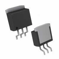
LM1085IS-3.3/NOPB National Semiconductor, LM1085IS-3.3/NOPB Datasheet - Page 9

LM1085IS-3.3/NOPB
Manufacturer Part Number
LM1085IS-3.3/NOPB
Description
IC REG POSITIVE 3A LDO TO-263
Manufacturer
National Semiconductor
Type
Voltage Regulatorr
Specifications of LM1085IS-3.3/NOPB
Regulator Topology
Positive Fixed
Voltage - Output
3.3V
Voltage - Dropout (typical)
1.3V @ 3A
Number Of Regulators
1
Current - Output
3A
Current - Limit (min)
3.2A
Operating Temperature
-40°C ~ 125°C
Mounting Type
Surface Mount
Package / Case
TO-263-3, D²Pak (3 leads + Tab), TO-263AA
Voltage Regulator Type
Linear
Topology
LDO
Regulator Output Type
Fixed
Polarity Type
Positive
Number Of Outputs
Single
Input Voltage (min)
2.6V
Input Voltage (max)
27V
Output Voltage
3.3V
Package Type
TO-263
Output Current
3A
Load Regulation
15mV
Line Regulation
6mV
Operating Temp Range
-40C to 125C
Operating Temperature Classification
Automotive
Dropout Voltage@current (max)
1.5@3A
Dropout Voltage@current (typ)
1.3@3A
Pin Count
3 +Tab
Mounting
Surface Mount
Quiescent Current (max)
10mA
Current, Output
3 A
Current, Supply
5 mA
Regulation, Line
1 mV
Regulation, Load
7 mV
Regulator Type
Low Dropout
Resistance, Thermal, Junction To Case
0.7 °C/W (Control Section), 3 °C/W (Output Section)
Temperature, Operating, Range
-40 to +125 °C
Voltage, Dropout
1.3 V
Voltage, Input
27 V
Voltage, Noise
0.003 %
Voltage, Output
3.3 V
Lead Free Status / RoHS Status
Lead free / RoHS Compliant
Voltage - Input
-
Lead Free Status / Rohs Status
Compliant
Other names
*LM1085IS-3.3
*LM1085IS-3.3/NOPB
LM1085IS-3.3
*LM1085IS-3.3/NOPB
LM1085IS-3.3
Available stocks
Company
Part Number
Manufacturer
Quantity
Price
Part Number:
LM1085IS-3.3/NOPB
Manufacturer:
NS/国半
Quantity:
20 000
Application Note
must be added, one for case to heat-sink (θ
heatsink to ambient (θ
predicted as follows:
T
T
P
consumption is calculated as follows:
Once the devices power is determined, the maximum allow-
able (θ
θ
The LM1085 has different temperature specifications for two
different sections of the IC: the control section and the output
section. The Electrical Characteristics table shows the junc-
tion to case thermal resistances for each of these sections,
while the maximum junction temperatures (T
section is listed in the Absolute Maximum section of the
datasheet. T
T
θ
follows:
θ
θ
The required heat sink is determined by calculating its re-
quired thermal resistance (θ
JA(max)
JA(max)
JA
JA
J
J
J(max)
D
= T
is junction temperature, T
(max, OUTPUT SECTION) = (150˚C - T
is the power consumption of the device. Device power
(max, CONTROL SECTION) = (125˚C - T
A
JA(max)
is 150˚C for the output section.
+ P
= T
should be calculated separately for each section as
D
R(max)
J(max)
) is calculated as:
(θ
JC
/P
+ θ
is 125˚C for the control section, while
D
= T
CH
HA
). The junction temperature can be
+ θ
J(max
HA(max)
HA
A
(Continued)
− T
) = T
is ambient temperature, and
A(max)
).
A
FIGURE 7. Heat sink thermal Resistance vs Area
+ P
)/P
D
D
FIGURE 6. Power Dissipation Diagram
θ
A(max)
CH
JA
J(max)
A(max)
) and one for
)/P
) for each
)/P
D
D
9
Figure 6 shows the voltages and currents which are present
in the circuit.
θ
θ
θ
TROL SECTION) + θ
θ
SECTION) + θ
If thermal compound is used, θ
C/W. If the case is soldered to the heat sink, then a θ
be estimated as 0 C/W.
After, θ
lower of the two θ
heat sink.
If PC board copper is going to be used as a heat sink, then
Figure 7 can be used to determine the appropriate area
(size) of copper foil required.
HA(max)
HA(max)
HA(max)
HA(max)
I
P
IN
D
= I
HA(max)
= (V
=θ
= θ
should also be calculated twice as follows:
= θ
L
JA
10094764
+ I
JA(max)
IN
JA
(max, OUTPUT SECTION) - (θ
−V
G
CH
is calculated for each section, choose the
(max, CONTROL SECTION) - (θ
OUT
)
HA(max)
− (θ
10094716
) I
CH
L
JC
)
+ V
values to determine the appropriate
+ θ
IN
CH
I
G
CH
)
can be estimated at 0.2
JC
www.national.com
(OUTPUT
JC
CH
(CON-
can


