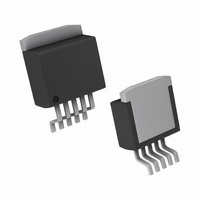
LP38501TS-ADJ/NOPB National Semiconductor, LP38501TS-ADJ/NOPB Datasheet - Page 5

LP38501TS-ADJ/NOPB
Manufacturer Part Number
LP38501TS-ADJ/NOPB
Description
IC REG LDO 3A FLEXCAP TO263-5
Manufacturer
National Semiconductor
Specifications of LP38501TS-ADJ/NOPB
Regulator Topology
Positive Adjustable
Voltage - Output
0.6 ~ 5 V
Voltage - Input
2.7 ~ 5.5 V
Voltage - Dropout (typical)
0.42V @ 3A
Number Of Regulators
1
Current - Output
3A
Operating Temperature
-40°C ~ 125°C
Mounting Type
Surface Mount
Package / Case
TO-263-5, D²Pak (5 leads + Tab), TO-263BA
Number Of Outputs
1
Polarity
Positive
Input Voltage Max
5.5 V
Output Voltage
0.6 V to 5 V
Output Type
Adjustable
Dropout Voltage (max)
0.55 V At 3 A
Output Current
3 A
Line Regulation
0.04 %/V
Load Regulation
0.12 %/A
Voltage Regulation Accuracy
+/- 3.5 %
Maximum Operating Temperature
+ 125 C
Mounting Style
SMD/SMT
Minimum Operating Temperature
- 40 C
For Use With
LP38501TS-ADJEV - 3A FLEXCAP LOW DROPOUT LINEAR RE
Lead Free Status / RoHS Status
Lead free / RoHS Compliant
Current - Limit (min)
-
Lead Free Status / Rohs Status
Details
Other names
LP38501TS-ADJ
Available stocks
Company
Part Number
Manufacturer
Quantity
Price
Company:
Part Number:
LP38501TS-ADJ/NOPB
Manufacturer:
TI
Quantity:
75
www.national.com
Enable Input (LP38501 Only)
ΔV
ΔV
Absolute Maximum Ratings
If Military/Aerospace specified devices are required,
please contact the National Semiconductor Sales Office/
Distributors for availability and specifications.
Electrical Characteristics
LP38501/3–ADJ
Unless otherwise specified: V
are for T
Maximum limits are guaranteed through test, design, or statistical correlation. Typical values represent the most likely parametric
norm at T
Storage Temperature Range
Lead Temperature
ESD Rating
Power
Input Pin Voltage (Survival)
Enable Pin Voltage (Survival)
Output Pin Voltage (Survival)
I
I
Symbol
OUT
DISABLED
I
OUT
V
V
OUT(PK)
OUT
I
I
V
V
(Soldering, 5 sec.)
I
t
t
IH(EN)
V
IL(EN)
I
IH(EN)
GND
IL(EN)
d(off)
d(on)
I
ADJ
ADJ
ADJ
SC
DO
(Survival)
/ΔI
/ΔV
Dissipation(Note
OUT
J
IN
J
= 25°C only; limits in boldface type apply over the junction temperature (T
= 25°C, and are provided for reference purposes only.
(Note
Adjust Pin Voltage
Adjust Pin Voltage
"A" GRADE
Adjust Pin Bias Current
Dropout Voltage
Output Voltage Line
Regulation
(Note
Output Voltage Load
Regulation
(Note
Ground Pin Current In Normal
Operation Mode
Ground Pin Current
Peak Output Current
Short Circuit Current
Enable Logic High
Enable Logic Low
Turn-off delay
Turn-on delay
Enable Pin High Current
Enable Pin Low Current
2)
4,
5,
Note
Note
Parameter
3)
6)
6)
IN
(Note
= 3.3V, I
(Note
(Note
7)
6)
6)
OUT
−65°C to +150°C
Internally Limited
Internally Limited
−0.3V to +6.0V
−0.3V to +6.0V
−0.3V to +6.0V
= 10 mA, C
2.7V
10 mA
2.7V
10 mA
2.7V
I
2.7V
10 mA
10 mA
V
V
V
V
V
Time from V
OFF
I
Time from V
ON
I
V
V
OUT
LOAD
LOAD
EN
OUT
OUT
OUT
OUT
EN
EN
(Note
< V
= V
= 0V
= 3A
≤
≤
≤
≤
≥
= 0V
= ON
= OFF
= 3A
= 3A
≤
≤
≤
≤
V
V
V
V
260°C
IL(EN)
V
IN
1)
±2 kV
IN
IN
IN
IN
OUT(NOM)
I
I
I
I
OUT
OUT
OUT
OUT
IN
≤
≤
≤
≤
Conditions
EN
EN
= 10 µF, C
5.5V
5.5V
5.5V
5.5V
≤
≤
≤
≤
< V
>V
3A
3A
3A
3A
IH(EN)
4
- 5%
IL(EN)
Operating Ratings
OUT
Input Supply Voltage
Enable Input Voltage
Output Current (DC)
Junction
V
to V
to V
OUT
= 10 µF, V
OUT
OUT
=
=
Temperature(Note
EN
0.584
0.575
0.596
0.587
J
Min
) range of -40°C to +125°C. Minimum and
3.5
1.4
—
—
—
—
—
—
—
—
—
= V
IN
, V
OUT
0.605
0.605
0.025
3)
0.04
0.05
0.12
0.24
Typ
420
= 1.8V. Limits in standard type
50
25
25
35
35
—
—
2
6
6
(Note
1)
0.626
0.635
0.614
0.623
0.125
Max
0.65
750
550
665
−40°C to +125°C
15
—
—
—
—
—
—
—
4
5
2.7V to 5.5V
0.0V to 5.5V
0.6V to 5V
0 to 3A
Units
%/V
%/A
mV
mA
nA
µA
nA
µs
V
V
A
A
V


