NCP584LSN18T1G ON Semiconductor, NCP584LSN18T1G Datasheet - Page 2
NCP584LSN18T1G
Manufacturer Part Number
NCP584LSN18T1G
Description
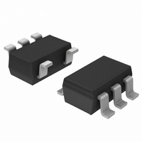
IC REG LDO 200MA 1.8V SOT23-5
Manufacturer
ON Semiconductor
Datasheet
1.NCP584HSN09T1G.pdf
(14 pages)
Specifications of NCP584LSN18T1G
Regulator Topology
Positive Fixed
Voltage - Output
1.8V
Voltage - Input
Up to 6V
Voltage - Dropout (typical)
0.2V @ 200mA
Number Of Regulators
1
Current - Output
200mA (Min)
Operating Temperature
-40°C ~ 85°C
Mounting Type
Surface Mount
Package / Case
SOT-23-5, SC-74A, SOT-25
Number Of Outputs
1
Polarity
Positive
Input Voltage Max
6 V
Output Voltage
1.8 V
Output Type
Fixed
Dropout Voltage (max)
0.3 V at 200 mA
Output Current
200 mA
Line Regulation
0.3 % / V
Load Regulation
40 mV
Voltage Regulation Accuracy
3 %
Maximum Power Dissipation
0.25 W
Maximum Operating Temperature
+ 85 C
Mounting Style
SMD/SMT
Minimum Operating Temperature
- 40 C
Lead Free Status / RoHS Status
Lead free / RoHS Compliant
Current - Limit (min)
-
Lead Free Status / Rohs Status
Details
Other names
NCP584LSN18T1GOSTR
Available stocks
Company
Part Number
Manufacturer
Quantity
Price
Company:

Part Number:
NCP584LSN18T1G
Manufacturer:
ON Semiconductor
Quantity:
1 750
Part Number:
NCP584LSN18T1G
Manufacturer:
ON/安森美
Quantity:
20 000


Stresses exceeding Maximum Ratings may damage the device. Maximum Ratings are stress ratings only. Functional operation above the
Recommended Operating Conditions is not implied. Extended exposure to stresses above the Recommended Operating Conditions may affect
device reliability.
PIN FUNCTION DESCRIPTION
MAXIMUM RATINGS
Input Voltage
Input Voltage (CE or CE Pin)
Input Voltage (ECO Pin)
Output Voltage
Output Current
Power Dissipation
ESD Capability, Human Body Model, C = 100 pF, R = 1.5 kW
ESD Capability, Machine Model, C = 200 pF, R = 0 W
Operating Ambient Temperature Range
Maximum Junction Temperature
Storage Temperature Range
SOT23−5
1
2
3
4
5
Pin Name
CE or CE
GND
ECO
V out
V
in
Rating
Power supply input voltage.
Power supply ground.
Chip enable pin.
Mode alternative pin. (V
Regulated output voltage.
http://onsemi.com
2
ECO
= V
in
for FT mode; V
ESD
Symbol
ESD
Description
T
V
J(max)
V
V
T
V
I
P
ECO
T
out
stg
CE
out
in
A
D
HBM
MM
ECO
= GND for LP mode)
−0.3 to V
−0.3 to V
−0.3 to V
−55 to +150
−40 to +85
Value
1000
250
250
150
125
6.5
in
in
in
+0.3
+0.3
+0.3
Unit
mW
mA
°C
°C
°C
V
V
V
V
V
V
Related parts for NCP584LSN18T1G
Image
Part Number
Description
Manufacturer
Datasheet
Request
R

Part Number:
Description:
Tri-Mode 200 mA CMOS LDO Regulator
Manufacturer:
ON Semiconductor
Datasheet:
Part Number:
Description:
ON Semiconductor [VOLTAGE REGULATOR]
Manufacturer:
ON Semiconductor
Datasheet:
Part Number:
Description:
357-036-542-201 CARDEDGE 36POS DL .156 BLK LOPRO
Manufacturer:
ON Semiconductor
Datasheet:
Part Number:
Description:
357-036-542-201 CARDEDGE 36POS DL .156 BLK LOPRO
Manufacturer:
ON Semiconductor
Datasheet:
Part Number:
Description:
357-036-542-201 CARDEDGE 36POS DL .156 BLK LOPRO
Manufacturer:
ON Semiconductor
Datasheet:
Part Number:
Description:
357-036-542-201 CARDEDGE 36POS DL .156 BLK LOPRO
Manufacturer:
ON Semiconductor
Datasheet:
Part Number:
Description:
357-036-542-201 CARDEDGE 36POS DL .156 BLK LOPRO
Manufacturer:
ON Semiconductor
Datasheet:
Part Number:
Description:
357-036-542-201 CARDEDGE 36POS DL .156 BLK LOPRO
Manufacturer:
ON Semiconductor
Datasheet:
Part Number:
Description:
357-036-542-201 CARDEDGE 36POS DL .156 BLK LOPRO
Manufacturer:
ON Semiconductor
Datasheet:
Part Number:
Description:
357-036-542-201 CARDEDGE 36POS DL .156 BLK LOPRO
Manufacturer:
ON Semiconductor
Datasheet:
Part Number:
Description:
357-036-542-201 CARDEDGE 36POS DL .156 BLK LOPRO
Manufacturer:
ON Semiconductor
Datasheet:
Part Number:
Description:
357-036-542-201 CARDEDGE 36POS DL .156 BLK LOPRO
Manufacturer:
ON Semiconductor
Datasheet:
Part Number:
Description:
Manufacturer:
ON Semiconductor
Datasheet:
Part Number:
Description:
Manufacturer:
ON Semiconductor
Datasheet: