NCP698SQ25T1G ON Semiconductor, NCP698SQ25T1G Datasheet
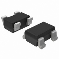
IC REG LDO 150MA 2.5V SC-82AB

NCP698SQ25T1G

Manufacturer Part Number
NCP698SQ25T1G
Description
IC REG LDO 150MA 2.5V SC-82AB
Manufacturer
ON Semiconductor
Datasheet

Specifications of NCP698SQ25T1G

Regulator Topology
Positive Fixed
Voltage - Output
2.5V
Voltage - Input
Up to 6V
Voltage - Dropout (typical)
0.52V @ 150mA
Number Of Regulators
1
Current - Output
150mA (Min)
Operating Temperature
-40°C ~ 85°C
Mounting Type
Surface Mount
Package / Case
SC-70-4, SC-82-4, SOT-323-4, SOT-343
Lead Free Status / RoHS Status
Lead free / RoHS Compliant
Current - Limit (min)
-
Other names
NCP698SQ25T1G
NCP698SQ25T1GOSTR

Available stocks

Company
Part Number
Manufacturer
Quantity
Price
Part Number:
NCP698SQ25T1G
Manufacturer:
ON
Quantity:
12 000
Part Number:
NCP698SQ25T1G
Manufacturer:
ON
Quantity:
36 000
Part Number:
NCP698SQ25T1G
Manufacturer:
ON
Quantity:
8 000
Company:
Part Number:
NCP698SQ25T1G
Quantity:
27 000
NCP698
150 mA CMOS Ultra Low Iq
and I
with Enable
designed for handheld communication equipment and portable battery
powered applications which require low quiescent and ground current.
This series features an ultra−low quiescent current of 2.5 mA. Each
device contains a voltage reference unit, an error amplifier, a PMOS
power transistor, resistors for setting output voltage, current limit, and
temperature limit protection circuits. The NCP698 series provides an
enable pin for ON/OFF control.
capacitors and requires a minimum output capacitor of 0.1 mF. The
device is housed in the micro−miniature SC82−AB surface mount
package. Standard voltage versions are 1.3, 1.5, 1.8, 2.5, 2.8, 3.0, 3.3,
3.5 and 5.0 V. Other voltages are available in 100 mV steps.
Features
Typical Applications
© Semiconductor Components Industries, LLC, 2009
March, 2009 − Rev. 1
This series of fixed output low−dropout linear regulators are
The NCP698 has been designed to be used with low cost ceramic
Ultra Low Quiescent Current of 2.5 mA Typical
Output Voltage Accuracy of 2.0%
Operating Temperature Range of −40°C to 85°C
Enable Function
This is a Pb−Free Device
Battery Powered Instruments
Hand−Held Instruments
Camcorders and Cameras
Input
C1
Figure 1. Typical Application Diagram
This device contains 28 active transistors
+
GND
GND Enable
V
LDO Regulator
in
V
out
OFF
ON
+
C2
Output
1
See detailed ordering and shipping information in the package
dimensions section on page 8 of this data sheet.
*Date Code orientation and/or position and
underbar may vary depending upon manu-
facturing location.
(Note: Microdot may be in either location)
xxx
M
G
ORDERING INFORMATION
GND
MARKING DIAGRAMS
PIN CONNECTIONS &
V
in
http://onsemi.com
SC82−AB (SC70−4)
= Specific Device Code
= Month Code*
= Pb−Free Package
1
2
4
CASE 419C
SQ SUFFIX
Top View)
Publication Order Number:
1
4
3
Enable
V
out
NCP698/D

Related parts for NCP698SQ25T1G

NCP698SQ25T1G Summary of contents

Page 1

NCP698 150 mA CMOS Ultra Low Iq and I LDO Regulator GND with Enable This series of fixed output low−dropout linear regulators are designed for handheld communication equipment and portable battery powered applications which require low quiescent and ground current. ...

Page 2

PIN FUNCTION DESCRIPTION Á Á Á Á ...

Page 3

ELECTRICAL CHARACTERISTICS ( 1 1.0 mF out(nom.) enable in in Characteristic Output Voltage (I = 1.0 mA) out 1.3 V 1.5 V 1.8 V 2.5 V 2.8 V ...

Page 4

ELECTRICAL CHARACTERISTICS ( 1 out(nom.) enable in in Enable Input Threshold Voltage (Voltage Increasing, Output Turns On, Logic High) (Voltage Decreasing, Output Turns Off, Logic Low) Output Voltage Temperature Coefficient ...

Page 5

3.0 V 2.7 OUT OUT 2.5 2.3 2.1 1.9 1.7 −60 −40 − TEMPERATURE (°C) Figure 2. Quiescent Current versus Temperature 3.020 3.015 3.010 ...

Page 6

V = 3.0 V OUT C = 0.1 mF −0.5 OUT OUT − 100 150 200 250 t, TIME (ms) Figure 8. Line Transient Response 60 30 ...

Page 7

A typical application circuit for the NCP698 is shown in Figure 1. Input Decoupling (C1) A 1.0 mF capacitor either ceramic or tantalum is recommended and should be connected close to the NCP698 package. Higher values and lower ESR will ...

Page 8

... ORDERING INFORMATION Nominal Output Voltage Device NCP698SQ13T1G NCP698SQ15T1G NCP698SQ18T1G NCP698SQ25T1G NCP698SQ28T1G NCP698SQ30T1G NCP698SQ33T1G NCP698SQ35T1G NCP698SQ50T1G †For information on tape and reel specifications, including part orientation and tape sizes, please refer to our Tape and Reel Packaging Specifications Brochure, BRD8011/D. Marking 1.3 LJW 1.5 LJX 1 ...

Page 9

... *For additional information on our Pb−Free strategy and soldering details, please download the ON Semiconductor Soldering and Mounting Techniques Reference Manual, SOLDERRM/D. ON Semiconductor and are registered trademarks of Semiconductor Components Industries, LLC (SCILLC). SCILLC reserves the right to make changes without further notice to any products herein. SCILLC makes no warranty, representation or guarantee regarding the suitability of its products for any particular purpose, nor does SCILLC assume any liability arising out of the application or use of any product or circuit, and specifically disclaims any and all liability, including without limitation special, consequential or incidental damages. “ ...

Related keywords