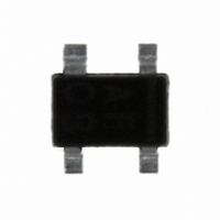
NCP580SQ15T1G ON Semiconductor, NCP580SQ15T1G Datasheet

NCP580SQ15T1G
Specifications of NCP580SQ15T1G
NCP580SQ15T1GOSTR
NCP580SQ15T1OSTR
NCP580SQ15T1OSTR
Available stocks
Related parts for NCP580SQ15T1G
NCP580SQ15T1G Summary of contents
Page 1
NCP580 Ultra-Fast, Low Noise 120 mA CMOS LDO Regulator with Enable The NCP580 series of low dropout regulators are designed for portable battery powered applications which require precise output voltage accuracy, low quiescent current, and high ripple rejection. These devices ...
Page 2
PIN FUNCTION DESCRIPTION Pin Symbol 1 Regulated output voltage. V out 2 GND Power supply ground Chip enable pin Power supply input voltage. in MAXIMUM RATINGS Rating Input Voltage Input Voltage (CE Pin) Output Voltage Output ...
Page 3
1.0 0.8 0.6 0.4 0 100 150 200 OUTPUT CURRENT I out Figure 2. Output Voltage vs. Output Current 1.6 1.5 1 1.0 mA out 1.3 I ...
Page 4
TEMPERATURE (°C) Figure 8. Output Voltage vs. Temperature 120 110 100 -50 0 TEMPERATURE (°C) Figure 10. Quiescent Current vs. Temperature 1.2 1.0 ...
Page 5
I = 1.0 mA out out out 2.5 Vdc + 0.5 Vp Ceramic 2 out 0 10 ...
Page 6
NCP580 TYPICAL CHARACTERISTICS C out 2.83 2.82 Input Voltage 2.81 2.80 2.79 Output Voltage 2.78 2. TIME, t (ms) C out 2.83 2.82 Input Voltage 2.81 2.80 2.79 Output Voltage 2.78 2. ...
Page 7
NCP580 TYPICAL CHARACTERISTICS C out 3.00 2.95 Output Current 2.90 2.85 Output Voltage 2.80 2.75 2. TIME, t (ms) C out 3.00 2.95 Output Current 2.90 2.85 Output Voltage 2.80 2.75 2. ...
Page 8
... GND. For PCB layout in considerations, the traces of V and GND should be in sufficiently wide in order to minimize noise and prevent unstable operation. ORDERING INFORMATION Device Output Type / Features NCP580SQ15T1G Active High NCP580SQ18T1G Active High NCP580SQ25T1G Active High NCP580SQ28T1G Active High NCP580SQ30T1G Active High ...
Page 9
... F L *For additional information on our Pb-Free strategy and soldering details, please download the ON Semiconductor Soldering and Mounting Techniques Reference Manual, SOLDERRM/D. ON Semiconductor and are registered trademarks of Semiconductor Components Industries, LLC (SCILLC). SCILLC reserves the right to make changes without further notice to any products herein. SCILLC makes no warranty, representation or guarantee regarding the suitability of its products for any particular purpose, nor does SCILLC assume any liability arising out of the application or use of any product or circuit, and specifically disclaims any and all liability, including without limitation special, consequential or incidental damages. “ ...


