LM337TG ON Semiconductor, LM337TG Datasheet - Page 2
LM337TG
Manufacturer Part Number
LM337TG
Description
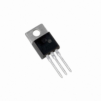
IC REG NEG 1.5A ADJ TO220AB
Manufacturer
ON Semiconductor
Datasheet
1.LM337BD2TR4G.pdf
(10 pages)
Specifications of LM337TG
Regulator Topology
Negative Adjustable
Voltage - Output
-1.2 ~ -37 V
Voltage - Input
Down to -40V
Number Of Regulators
1
Current - Output
500mA
Operating Temperature
0°C ~ 125°C
Mounting Type
Through Hole
Package / Case
TO-220-3 (Straight Leads)
Polarity
Negative
Number Of Outputs
1
Output Type
Adjustable
Output Voltage
- 1.2 V to - 37 V
Output Current
1.5 A
Line Regulation
0.04 % / V
Load Regulation
1 % / V
Input Voltage Max
- 40 V
Maximum Operating Temperature
+ 125 C
Minimum Operating Temperature
0 C
Mounting Style
Through Hole
Reference Voltage
- 1.25 V
Lead Free Status / RoHS Status
Lead free / RoHS Compliant
Voltage - Dropout (typical)
-
Current - Limit (min)
-
Lead Free Status / Rohs Status
Lead free / RoHS Compliant
Other names
LM337TGOS
Available stocks
Company
Part Number
Manufacturer
Quantity
Price

Part Number:
LM337TG
Manufacturer:
ON/安森美
Quantity:
20 000


Stresses exceeding Maximum Ratings may damage the device. Maximum Ratings are stress ratings only. Functional operation above the
Recommended Operating Conditions is not implied. Extended exposure to stresses above the Recommended Operating Conditions may affect
device reliability.
1. T
2. I
3. Load and line regulation are specified at constant junction temperature. Change in V
4. C
5. Power dissipation within an IC voltage regulator produces a temperature gradient on the die, affecting individual IC components on the die.
6. Since Long Term Stability cannot be measured on each device before shipment, this specification is an engineering estimate of average
MAXIMUM RATINGS
ELECTRICAL CHARACTERISTICS
Input−Output Voltage Differential
Power Dissipation
Operating Junction Temperature Range
Storage Temperature Range
Line Regulation (Note 3), T
Load Regulation (Note 3), T
Thermal Regulation, T
Adjustment Pin Current
Adjustment Pin Current Change, 2.5 V ≤ |V
Reference Voltage, T
Line Regulation (Note 3), 3.0 V ≤ |V
Load Regulation (Note 3), 10 mA ≤ I
Temperature Stability (T
Minimum Load Current to Maintain Regulation
Maximum Output Current
RMS Noise, % of V
Ripple Rejection, V
Long−Term Stability, T
Thermal Resistance, Junction−to−Case, T Package
Thermal Regulation specification. Pulse testing with a low duty cycle is used.
These effects can be minimized by proper integrated circuit design and layout techniques. Thermal Regulation is the effect of these
temperature gradients on the output voltage and is expressed in percentage of output change per watt of power change in a specified time.
stability from lot to lot.
max
low
Adj
, when used, is connected between the adjustment pin and ground.
Case 221A
Case 936 (D
to T
= 1.5 A, P
|V
|V
10 mA ≤ I
10 mA ≤ I
|V
|V
(|V
(|V
|V
|V
Without C
C
Endpoint Measurements
high
Adj
O
O
O
O
I
I
−V
−V
I
I
−V
−V
| ≤ 5.0 V
| ≥ 5.0 V
| ≤ 5.0 V
| ≥ 5.0 V
= 0° to +125°C, for LM337T, D2T.
= 10 mF
O
O
O
O
max
T
Thermal Resistance, Junction−to−Ambient
Thermal Resistance, Junction−to−Case
T
Thermal Resistance, Junction−to−Ambient
Thermal Resistance, Junction−to−Case
| ≤ 15 V, P
| ≤ 40 V, P
| ≤ 10 V)
| ≤ 40 V)
A
A
O
O
2
L
O
= +25°C
= +25°C
Adj
PAK)
, T
= 20 W
= −10 V, f = 120 Hz (Note 4)
≤ I
A
≤ I
A
J
A
= +25°C, 3.0 V ≤ |V
low
= T
= +25°C (Note 5), 10 ms Pulse
max
max
(T
= +25°C, 10 Hz ≤ f ≤ 10 kHz
A
A
D
D
high
, P
≤ T
A
Characteristics
, P
= +25°C, unless otherwise noted)
= +25°C, 3.0 V ≤ |V
≤ P
≤ P
= +25°C, 10 mA ≤ I
D
D
J
(Note 6), T
≤ T
≤ P
≤ P
max
max
high
max
I
max
−V
O
, T Package
, T
≤ I
Rating
O
)
J
, T
, T
| ≤ 40 V
= +25°C, T Package
max
A
A
J
(|V
I
I
= +25°C
−V
−V
= T
= +25°C for
I−
O
O
V
low
| ≤ 40 V,
| ≤ 40 V,
O
I
−V
O
| = 5.0 V; I
to T
≤ I
T
O
low
| ≤ 40 V
max
high
to T
http://onsemi.com
O
high
= 0.5 A for T package; T
= − 40° to +125°C, for LM337BT, BD2T.
LM337
2
Figure
1, 2
1
2
3
3
1
2
3
3
3
4
3
J
= T
O
Reg
Symbol
Symbol
Reg
Reg
Reg
Reg
V
because of heating effects is covered under the
DI
R
I
I
T
low
q
q
q
q
I
V
Lmin
I
RR
P
P
max
T
T
−V
Adj
N
qJC
stg
S
JC
JC
JA
JA
ref
therm
Adj
D
D
S
J
load
load
line
line
to T
O
high
−1.21
−1.20
[Note 1]; I
Min
66
−
−
−
−
−
−
3
−
−
−
−
−
−
−
−
−
−
−
−
Internally Limited
Internally Limited
−40 to +125
−65 to +150
Value
0.003
−1.25
−1.25
0.003
0.01
0.02
0.15
Typ
5.0
5.0
0.3
2.0
0.3
0.6
1.5
2.5
1.5
0.3
4.0
40
65
70
15
65
20
60
77
max
0
and P
−1.28
−1.30
Max
0.04
0.04
0.07
100
1.0
5.0
1.5
6.0
2.2
0.4
1.0
50
70
10
7
−
−
−
−
−
max
[Note 2].)
% V
%/1.0 k
°C/W
°C/W
°C/W
°C/W
% V
% V
% V
% V
°C/W
Unit
Unit
%/V
%/V
Hrs.
Vdc
mV
mV
mA
mA
mA
dB
°C
°C
W
W
V
A
O
O
O
O
O
/W
Related parts for LM337TG
Image
Part Number
Description
Manufacturer
Datasheet
Request
R

Part Number:
Description:
1.5 A, Adjustable Output, Negative Voltage Regulat
Manufacturer:
On Semiconductor
Part Number:
Description:
ON Semiconductor [VOLTAGE REGULATOR]
Manufacturer:
ON Semiconductor
Datasheet:
Part Number:
Description:
357-036-542-201 CARDEDGE 36POS DL .156 BLK LOPRO
Manufacturer:
ON Semiconductor
Datasheet:
Part Number:
Description:
357-036-542-201 CARDEDGE 36POS DL .156 BLK LOPRO
Manufacturer:
ON Semiconductor
Datasheet:
Part Number:
Description:
357-036-542-201 CARDEDGE 36POS DL .156 BLK LOPRO
Manufacturer:
ON Semiconductor
Datasheet:
Part Number:
Description:
357-036-542-201 CARDEDGE 36POS DL .156 BLK LOPRO
Manufacturer:
ON Semiconductor
Datasheet:
Part Number:
Description:
357-036-542-201 CARDEDGE 36POS DL .156 BLK LOPRO
Manufacturer:
ON Semiconductor
Datasheet:
Part Number:
Description:
357-036-542-201 CARDEDGE 36POS DL .156 BLK LOPRO
Manufacturer:
ON Semiconductor
Datasheet:
Part Number:
Description:
357-036-542-201 CARDEDGE 36POS DL .156 BLK LOPRO
Manufacturer:
ON Semiconductor
Datasheet:
Part Number:
Description:
357-036-542-201 CARDEDGE 36POS DL .156 BLK LOPRO
Manufacturer:
ON Semiconductor
Datasheet:
Part Number:
Description:
357-036-542-201 CARDEDGE 36POS DL .156 BLK LOPRO
Manufacturer:
ON Semiconductor
Datasheet:
Part Number:
Description:
357-036-542-201 CARDEDGE 36POS DL .156 BLK LOPRO
Manufacturer:
ON Semiconductor
Datasheet: