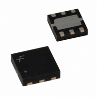
FAN1540BMPX Fairchild Semiconductor, FAN1540BMPX Datasheet - Page 7

FAN1540BMPX
Manufacturer Part Number
FAN1540BMPX
Description
IC REG LDO 1.3A 3.3V 6-MLP
Manufacturer
Fairchild Semiconductor
Datasheet
1.FAN1540BMPX.pdf
(9 pages)
Specifications of FAN1540BMPX
Regulator Topology
Positive Fixed
Voltage - Output
3.3V
Voltage - Input
Up to 10V
Voltage - Dropout (typical)
0.9V @ 1.3A
Number Of Regulators
1
Current - Output
1.3A
Operating Temperature
0°C ~ 125°C
Mounting Type
Surface Mount
Package / Case
6-MLP
Number Of Outputs
1
Polarity
Positive
Input Voltage Max
10 V
Output Voltage
3.3 V
Output Type
Fixed
Dropout Voltage (max)
1.2 V at 1300 mA
Output Current
1 A
Line Regulation
15 mV
Load Regulation
40 mV
Maximum Operating Temperature
+ 150 C
Mounting Style
SMD/SMT
Minimum Operating Temperature
0 C
Lead Free Status / RoHS Status
Lead free / RoHS Compliant
Current - Limit (min)
-
Lead Free Status / Rohs Status
Lead free / RoHS Compliant
Other names
FAN1540BMPXTR
Available stocks
Company
Part Number
Manufacturer
Quantity
Price
Company:
Part Number:
FAN1540BMPX
Manufacturer:
Fairchild Semiconductor
Quantity:
1 901
© 2007 Fairchild Semiconductor Corporation
FAN1539B / FAN1540B • Rev. 1.0.0
voltage, with an operating die (junction) temperature
of up to 125°C. Once the power dissipation and
thermal resistance are known, the maximum junction
temperature of the device can be calculated. While
the power dissipation is calculated from known
electrical parameters, the actual thermal resistance
depends on the thermal characteristics of the chosen
package and the surrounding PC board copper to
which it is mounted.
The power dissipation is equal to the product of the
input-to-output voltage differential and the output
current, plus the ground current, multiplied by the
input voltage:
Applications Information
General Circuit Description
The FAN1539B / FAN1540B is an advanced low-
dropout voltage regulator specially designed for
applications in portable computers, where high
performance and low quiescent current are required.
The device has an internal trimmed bandgap voltage
reference and an internal output voltage sense
divider. These two signals form the input to the error
amplifier that regulates the output voltage.
The FAN1539B / FAN1540B has a set of internal
protection circuitry, including thermal shutdown, short-
circuit current limit, and electrostatic discharge
protection. Low-ESR ceramic capacitors are needed
for input as well as output pins to maintain the circuit
stability.
Short-Circuit Current Limit
The device has internal over-current limit and short-
circuit protection. Under over-current conditions, the
device current is determined by the current-limit
threshold. Once the device is released from short-
circuit conditions, the normal level of current limit is
gradually re-established as the device output voltage
reaches normal levels. Special circuitry has been
added to ensure that recovery from short-circuit
current conditions does not lead to excessive
overshoot of the output voltage — a phenomenon
often encountered in conventional regulators.
Thermal Protection
The FAN1539B / FAN1540B is designed to supply at
least 1A/1.3A output current. Excessive output load at
high input-output voltage difference causes the device
temperature to increase and exceed maximum ratings
due to power dissipation. During output overload
conditions, if the die temperature exceeds the
shutdown limit temperature of 160°C, an onboard
thermal protection disables the output until the
temperature drops approximately 15°C below the limit;
at which point, the output is re-enabled.
Thermal Characteristics
The FAN1539/FAN1539B / FAN1540B is designed to
supply at least 1A/1.3A at the specified output
7
The ground pin current, I
Electrical Characteristics tables.
The relationship describing the thermal behavior of
the package is:
where T
temperature of the die, which is 150°C, and TA is the
ambient operating temperature. θ
the surrounding PC board layout and can be
empirically obtained. While the θ
of the 6-lead MLP package is specified at 8°C/W, the
θ
higher. This can be improved by providing a heat sink
of
Depending on the size of the copper area and the
thickness of the copper layer, the resulting θ
vary over a wide range. The addition of backside
copper with through-holes, stiffeners, and other
enhancements can also reduce thermal resistance.
Thermal simulations performed on a thermally
optimized board layout indicate that
20°C /W can be achieved.
The heat contributed by the dissipation of other
devices located nearby must be included in the design
considerations. Overload conditions also need to be
considered. It is possible for the device to enter a
thermal cycling loop, in which the circuit enters a
shutdown condition, cools, re-enables, and then again
overheats and shuts down repeatedly due to a
persistent fault condition.
Capacitor ESR and PCB Layout
The FAN1539/FAN1539B / FAN1540B has been
optimized
capacitors down to less than 0mΩ. For best results,
place both input and output bypass capacitors as near
to the input and output pins as possible. X7R types
are
GRM31CR70J106KA01B
GRM43ER71A226KE01B
component from TDK. The capacitors should connect
directly to the ground plane. Use of ground plane on
the top and the bottom side of the PCB is
recommended. As many vias as possible should be
used to minimize ground plane resistance.
JA
surrounding
for a minimum PWB footprint is substantially
J(max)
recommended,
to
is the maximum allowable junction
accommodate
copper
GND
ground
(22µF)
including
can be found in the
JC
JA
(10µF)
low-ESR
(junction-to-case)
is dependent on
on
θ
JA
or
www.fairchildsemi.com
the
as low as
Murata’s
bypass
JA
similar
EQ. 1
EQ. 2
PWB.
and
can


