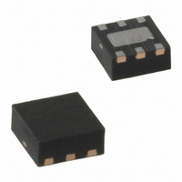
MIC5219YMT TR Micrel Inc, MIC5219YMT TR Datasheet - Page 12

MIC5219YMT TR
Manufacturer Part Number
MIC5219YMT TR
Description
IC REG LDO 500MA ADJ VOLT 6TMLF
Manufacturer
Micrel Inc
Datasheet
1.MIC5219-3.3YM5_TR.pdf
(14 pages)
Specifications of MIC5219YMT TR
Regulator Topology
Positive Adjustable
Voltage - Output
Adjustable
Voltage - Input
2.5 ~ 12 V
Voltage - Dropout (typical)
0.35V @ 500mA
Number Of Regulators
1
Current - Output
500mA
Operating Temperature
-40°C ~ 125°C
Mounting Type
Surface Mount
Package / Case
6-TMLF®, QFN
Lead Free Status / RoHS Status
Lead free / RoHS Compliant
Current - Limit (min)
-
Other names
576-3522-2
The power dissipation at 500mA must also be calculated.
This number must be multiplied by the duty cycle at which it
would be operating, 12.5%.
The total power dissipation of the device under these condi-
tions is the sum of the two power dissipation figures.
The total power dissipation of the regulator is less than the
maximum power dissipation of the SOT-23-5 package at room
temperature, on a minimum footprint board and therefore
would operate properly.
Multilayer boards with a ground plane, wide traces near the
pads, and large supply-bus lines will have better thermal
conductivity.
For additional heat sink characteristics, please refer to Mi-
crel “Application Hint 17, Designing P.C. Board Heat Sinks”,
included in Micrel’s Databook. For a full discussion of heat
sinking and thermal effects on voltage regulators, refer to
“Regulator Thermals” section of Micrel’s Designing with Low-
Dropout Voltage Regulators handbook.
Fixed Regulator Circuits
Figure 5 shows a basic MIC5219-x.xBMX fixed-voltage regu-
lator circuit. A 1µF minimum output capacitor is required for
basic fixed-voltage applications.
June 2009
Figure 5. Low-Noise Fixed Voltage Regulator
P
P
P
P
P
P
P
P
P
D
D
D
D
D
D
D(total)
D(total)
D(total)
× 50mA = 0.875 × 173mW
× 50mA = 151mW
× 500mA = (5V – 3.3V) 500mA + 5V × 20mA
× 500mA = 950mW
× = 0.125 × 950mW
× = 119mW
= P
= 151mW + 119mW
= 270mW
V
IN
D
× 50mA + P
MIC5219-x.x
IN
E N
GND
OUT
B Y P
D
× 500mA
1µF
V
OU T
12
Figure 6 includes the optional 470pF noise bypass capacitor
between BYP and GND to reduce output noise. Note that the
minimum value of C
capacitor is used.
Adjustable Regulator Circuits
Figure 7 shows the basic circuit for the MIC5219 adjustable
regulator. The output voltage is configured by selecting values
for R1 and R2 using the following formula:
Although ADJ is a high-impedance input, for best performance,
R2 should not exceed 470kΩ.
Figure 8 includes the optional 470pF bypass capacitor from
ADJ to GND to reduce output noise.
Figure 6. Ultra-Low-Noise Fixed Voltage Regulator
Figure 7. Low-Noise Adjustable Voltage Regulator
Figure 8. Ultra-Low-Noise Adjustable Application
V
OUT
V
IN
V
= 1.242V
V
IN
IN
IN
E N
MIC5219
IN
E N
MIC5219-x.x
OUT
IN
E N
GND
MIC5219
GND
R2
R1
GND
must be increased when the bypass
OUT
ADJ
+ 1
OUT
ADJ
470pF
OUT
B Y P
470pF
R 1
R 2
R 1
R 2
2.2µF
V
1µF
OU T
V
2.2µF
V
OU T
OU T
M0371-061809


