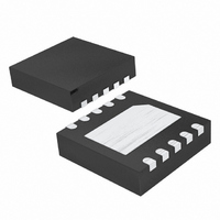
MAX15027ATB+T Maxim Integrated Products, MAX15027ATB+T Datasheet - Page 2

MAX15027ATB+T
Manufacturer Part Number
MAX15027ATB+T
Description
IC LDO REG ADJ 1A 10-TDFN
Manufacturer
Maxim Integrated Products
Datasheet
1.MAX15028ATBT.pdf
(11 pages)
Specifications of MAX15027ATB+T
Regulator Topology
Positive Adjustable
Voltage - Output
0.5 ~ 3.3 V
Voltage - Input
1.43 ~ 3.6 V
Voltage - Dropout (typical)
0.075V @ 1A
Number Of Regulators
1
Current - Output
1A
Current - Limit (min)
1.4A
Operating Temperature
-40°C ~ 125°C
Mounting Type
Surface Mount
Package / Case
10-TDFN Exposed Pad
Lead Free Status / RoHS Status
Lead free / RoHS Compliant
Other names
MAX15027ATB+T
MAX15027ATB+TTR
MAX15027ATB+TTR
ABSOLUTE MAXIMUM RATINGS
IN, FB, SS, I.C. to GND..........................................-0.3V to +4.0V
BIAS to GND.............................................................-0.3V to +6V
EN to GND ................-0.3V to the lower of (V
OUT to GND ................................................-0.3V to (V
Output Short-Circuit Duration.....................................Continuous
Continuous Power Dissipation (T
1.425V to 3.6V Input, 1A Low-Dropout
Regulators with BIAS Input
ELECTRICAL CHARACTERISTICS
(Circuit of Figure 1; V
+125°C. Typical values are at T
Stresses beyond those listed under “Absolute Maximum Ratings” may cause permanent damage to the device. These are stress ratings only, and functional
operation of the device at these or any other conditions beyond those indicated in the operational sections of the specifications is not implied. Exposure to
absolute maximum rating conditions for extended periods may affect device reliability.
2
Note 1: Package thermal resistances were obtained using the method described in JEDEC specification JESD51-7, using a four-
IN
Input Voltage Range
Undervoltage Lockout
Undervoltage Lockout Hysteresis
Quiescent GND Current
Input Supply Current in Shutdown
BIAS (MAX15028)
Input Voltage Range
Undervoltage Lockout
Undervoltage Lockout Hysteresis
Quiescent Input Supply Current
Input Supply Current in Shutdown
10-Pin TDFN, Multilayer Board
(derate 24.4mW/°C above +70°C) ..............................1951mW
_______________________________________________________________________________________
layer board. For detailed information on package thermal considerations, refer to www.maxim-ic.com/thermal-tutorial.
PARAMETER
IN
= 1.8V, V
A
A
= +25°C, unless otherwise noted.) (Note 2)
OUT
= +70°C)
V
V
SYMBOL
UVLO_HYST
= 1.2V, EN = IN for MAX15027, EN = BIAS for MAX15028, I
BIAS_UVLO
I
BIAS_SD
V
I
V
I
IN_SD
I
UVLO
GND
BIAS
V
BIAS
IN
BIAS
+ 0.3V) or +6V
MAX15027
MAX15028
V
I
V
I
V
V
V
V
I
V
EN = GND
OUT
OUT
OUT
IN
IN
IN
IN
EN
BIAS
EN
IN
rising,
= 1.425V to 3.6V, V
= 3.6V, V
= 3.3V, V
= 0V, T
= V
+ 0.3V)
= 2mA
= 1mA, V
= 2mA
rising, I
BIAS
A
OUT
OUT
= - 40°C to + 85°C
OUT
CONDITIONS
BIAS
= 3.3V, I
= 3.3V, I
= 2mA
Junction-to-Case Thermal Resistance, θ
Junction-to-Ambient Thermal Resistance, θ
Operating Junction Temperature Range ...........-40°C to +125°C
Maximum Junction Temperature .....................................+150°C
Storage Temperature Range .............................-65°C to +150°C
Lead Temperature (soldering, 10s) .................................+300°C
Soldering Temperature (reflow) .......................................+260°C
= 3.3V
V
V
V
V
V
V
V
BIAS = IN
MAX15027
MAX15028
IN
BIAS
I N
B I AS
I N
B I AS
BIAS
OUT
= 0V, V
= 3.3V , V
= 3.3V , V
OUT
OUT
= 3.3V
= 3.3V
= 5V
= 3V to 5.5V
= 1.2V,
= 100mA
= 500mA
OUT
OU T
OU T
= 0V,
= 0V ,
= 0V ,
1.425
1.425
3.000
1.275
1.04
MIN
160
180
170
2.3
20
OUT
3
= 100mA, T
1.325
1.106
TYP
275
275
315
110
0.1
2.5
1.2
1.2
1.5
50
60
JC
.......................9°C/W
JA
(Note 1)...41°C/W
A
3.600
3.600
3.600
1.375
MAX
1.14
410
560
470
120
5.5
5.5
2.7
= T
2
2
3
J
= -40°C to
UNITS
mV
mV
µA
µA
µA
µA
V
V
V
V


