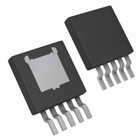
LP38501TJ-ADJ/NOPB National Semiconductor, LP38501TJ-ADJ/NOPB Datasheet - Page 11

LP38501TJ-ADJ/NOPB
Manufacturer Part Number
LP38501TJ-ADJ/NOPB
Description
IC REG LDO 3A FLEXCAP TO263T-5
Manufacturer
National Semiconductor
Datasheet
1.LP38501TJ-ADJNOPB.pdf
(18 pages)
Specifications of LP38501TJ-ADJ/NOPB
Regulator Topology
Positive Adjustable
Voltage - Output
0.6 ~ 5 V
Voltage - Input
2.7 ~ 5.5 V
Voltage - Dropout (typical)
0.42V @ 3A
Number Of Regulators
1
Current - Output
3A
Operating Temperature
-40°C ~ 125°C
Mounting Type
Surface Mount
Package / Case
TO-263-5 Thin
For Use With
LP38501TS-ADJEV - 3A FLEXCAP LOW DROPOUT LINEAR RE
Lead Free Status / RoHS Status
Lead free / RoHS Compliant
Current - Limit (min)
-
Other names
LP38501TJ-ADJ
LP38501TJ-ADJ
LP38501TJ-ADJTR
LP38501TJ-ADJ
LP38501TJ-ADJTR
www.national.com
The reduction in unity-gain bandwidth as load current is re-
duced is normal for any LDO regulator using a P-FET or PNP
pass transistor, because they have a pole in the loop gain
function given by:
This illustrates how the pole goes to the highest frequency
when R
eral, LDO’s have maximum bandwidth (and lowest phase
margin) at full load current. In the case of the LP38501, it can
be seen that it has good phase margin even when using ce-
ramic capacitors with ESR values of only a few milli Ohms.
LOAD TRANSIENT RESPONSE
Load transient response is defined as the change in regulated
output voltage which occurs as a result of a change in load
current. Many applications have loads which vary, and the
control loop of the voltage regulator must adjust the current
in the pass FET transistor in response to load current
changes. For this reason, regulators with wider bandwidths
often have better transient response.
The LP38501 employs an internal feedforward design which
makes the load transient response much faster than would be
predicted simply by loop speed: this feedforward means any
voltage changes appearing on the output are coupled through
to the high-speed driver used to control the gate of the pass
FET along a signal path using very fast FET devices. Because
of this, the pass transistor’s current can change very quickly.
Figure 4
a change in load current of 0.1A – 3A, and then 3A – 0.1A
with a load current slew rate of 500 mA/µs. As shown in the
plots, the resulting change in output voltage is only about 40
mV (peak), which is just slightly over 2% for the 1.8V output
used for this test. This is excellent performance for such a
small output capacitor.
FIGURE 3. Gain-Bandwidth Plot for No Load
L
shows the output transient response resulting from
is minimum value (maximum load current). In gen-
30028154
10
When the load current changes much more quickly, the output
voltage will show more change because the loop and internal
feedforward circuitry are not able to react as fast as the load
changes. In such cases, it is the output capacitor which must
supply load current during the transition until the loop re-
sponds and changes the pass transistor’s drive to deliver the
new value of load current. As an example, the slew rate of the
load current will be increased to 75A/µs and the same test will
be performed. In
cursion of the output voltage during the transient has now
increased to about 200 mV, which is just slightly over 11% for
the 1.8V output.
A better understanding of the load transient can be obtained
when the load’s rising edge is expanded in time scale
6).
FIGURE 4. Load Transient Response: 10 µF Ceramic,
FIGURE 5. Load Transient Response: 10 µF Ceramic,
Figure
0.5A/µs di/dt
75A/µs di/dt
5, it can be seen that the peak ex-
30028134
30028136
(Figure


