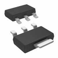
LM2940IMP-12/NOPB National Semiconductor, LM2940IMP-12/NOPB Datasheet - Page 14

LM2940IMP-12/NOPB
Manufacturer Part Number
LM2940IMP-12/NOPB
Description
IC REGULATOR LDO 1A SOT-223
Manufacturer
National Semiconductor
Datasheet
1.LM2940IMP-5.0NOPB.pdf
(20 pages)
Specifications of LM2940IMP-12/NOPB
Regulator Topology
Positive Fixed
Voltage - Output
12V
Voltage - Input
13.6 ~ 26 V
Voltage - Dropout (typical)
0.5V @ 1A
Number Of Regulators
1
Current - Output
1A
Operating Temperature
-40°C ~ 85°C
Mounting Type
Surface Mount
Package / Case
SOT-223 (3 leads + Tab), SC-73, TO-261
Voltage Regulator Type
Linear
Topology
LDO
Regulator Output Type
Fixed
Polarity Type
Positive
Number Of Outputs
Single
Input Voltage (min)
13.6V
Input Voltage (max)
26V
Output Voltage
12V
Package Type
SOT-223
Output Current
1(Typ)A
Load Regulation
120mV
Line Regulation
120mV
Operating Temp Range
-40C to 85C
Operating Temperature Classification
Industrial
Dropout Voltage@current (typ)
0.5@1A/0.11@100mA
Pin Count
3 +Tab
Mounting
Surface Mount
Quiescent Current (max)
15mA
Lead Free Status / RoHS Status
Lead free / RoHS Compliant
Current - Limit (min)
-
Lead Free Status / Rohs Status
Compliant
Other names
LM2940IMP-12
LM2940IMP-12TR
LM2940IMP-12TR
www.national.com
θ
When a value for θ
heatsink must be selected that has a value that is less than
or equal to this number.
θ
in the catalog, or shown in a curve that plots temperature rise
vs power dissipation for the heatsink.
HEATSINKING TO-263 PACKAGE PARTS
The TO-263 (“S”) package uses a copper plane on the PCB
and the PCB itself as a heatsink. To optimize the heat sinking
ability of the plane and PCB, solder the tab of the package to
the plane.
Figure 3 shows for the TO-263 the measured values of θ
for different copper area sizes using a typical PCB with 1
ounce copper and no solder mask over the copper area used
for heatsinking.
FIGURE 3. θ
As shown in the figure, increasing the copper area beyond 1
square inch produces very little improvement. It should also
be observed that the minimum value of θ
package mounted to a PCB is 32°C/W.
As a design aid, Figure 4 shows the maximum allowable pow-
er dissipation compared to ambient temperature for the
TO-263 device. This assumes a θ
inch of 1 ounce copper and a maximum junction temperature
(T
(H−A)
J
) of 125°C.
is specified numerically by the heatsink manufacturer
(C−H)
(JA)
is defined as the thermal resistance between
the case and the surface of the heatsink. The
value of θ
about 2.5°C/W (depending on method of at-
tachment, insulator, etc.). If the exact value is
unknown, 2°C/W should be assumed for θ
−H)
vs. Copper (1 ounce) Area for the TO-263
.
(H−A)
is found using the equation shown, a
(C−H)
Package
will vary from about 1.5°C/W to
(JA)
of 35°C/W for 1 square
(JA)
for the TO-263
882238
(JA)
(C
14
HEATSINKING SOT-223 PACKAGE PARTS
The SOT-223 (“MP”) packages use a copper plane on the
PCB and the PCB itself as a heatsink. To optimize the heat
sinking ability of the plane and PCB, solder the tab of the
package to the plane.
Figure 5 and Figure 6 show the information for the SOT-223
package. Figure 6 assumes a θ
inch of 1 ounce copper and 51°C/W for 1 square inch of 2
ounce copper, with a maximum ambient temperature (T
85°C and a maximum junction temperature (T
For techniques for improving the thermal resistance and pow-
er dissipation for the SOT-223 package, please refer to Ap-
plication Note AN-1028.
FIGURE 5. θ
FIGURE 4. Maximum Power Dissipation vs. T
(JA)
vs. Copper (2 ounce) Area for the SOT-223
TO-263 Package
Package
(JA)
of 74°C/W for 1 square
882240
J
) of 125°C.
882239
A
for the
A
) of


