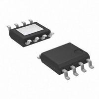
AP7173-SPG-13 Diodes Inc, AP7173-SPG-13 Datasheet - Page 5

AP7173-SPG-13
Manufacturer Part Number
AP7173-SPG-13
Description
IC REG LDO ADJ 1.5A 8SOIC
Manufacturer
Diodes Inc
Datasheet
1.AP7173-SPG-13.pdf
(15 pages)
Specifications of AP7173-SPG-13
Regulator Topology
Positive Adjustable
Voltage - Output
0.8 ~ 3.3 V
Voltage - Input
1 ~ 5.5 V
Voltage - Dropout (typical)
0.165V @ 1.5A
Number Of Regulators
1
Current - Output
1.5A (Max)
Current - Limit (min)
2A
Operating Temperature
-40°C ~ 85°C
Mounting Type
Surface Mount
Package / Case
8-SOIC (3.9mm Width) Exposed Pad, 8-eSOIC. 8-HSOIC
Lead Free Status / RoHS Status
Lead free / RoHS Compliant
Other names
AP7173-SPG-13
AP7173-SPG-13DITR
AP7173-SPG-13DITR
Available stocks
Company
Part Number
Manufacturer
Quantity
Price
Part Number:
AP7173-SPG-13
Manufacturer:
DIODES/美台
Quantity:
20 000
Company:
Part Number:
AP7173-SPG-13-80
Manufacturer:
CENTRAL
Quantity:
15 362
Electrical Characteristics
At V
unless otherwise noted. Typical values are at T
Notes:
AP7173
Document number: DS31369 Rev. 9 - 2
ΔV
ΔV
EN
Symbol
V
V
OUT
I
V
V
V
OUT
PSRR
/ΔI
I
V
PG, LKG
I
V
V
V
V
SHORT
EN, HYS
PG, HYS
= 1.1V, V
V
I
SHDN
PG, TH
PG, LO
T
EN, LO
T
V
EN, HI
θ
θ
I
I
I
VCC
I
VCC
OUT
OUT
REF
SS
EN
10. Test condition for DFN3030-10: Device mounted on FR-4 substrate (2s2p), 2"*2" PCB, with 2oz copper trace thickness and large pad pattern.
CL
FB
11. Test condition for SOP-8L-EP: Device mounted on FR-4 substrate (2s2p), 2"*2" PCB, with 2oz copper trace thickness and large pad pattern.
DO
OUT
ST
SD
JA
JC
IN
7. V
8. Tested at 0.8V; resistor tolerance is not taken into account.
9. Dropout is defined as the voltage from V
/ΔV
/V
OUT
VCC
IN
/
should be higher or equal to V
IN
Input Voltage Range
Bias Pin Voltage Range
(Note 7)
Internal Reference
(Adj.)
Output Voltage Range
Accuracy (Note 8)
Line Regulation
Load Regulation
Dropout Voltage
(Note 9)
Current Limit
Short-Circuit Current
Bias Pin Current
Shutdown Supply
Current (I
Feedback Pin Current
Power-Supply Rejection
(V
Power-SupplyRejection
(V
Startup Time
Soft-Start Charging
Current
Enable Input High Level
Enable Input Low Level
Enable Pin Hysteresis
Enable Pin Current
PG Trip Threshold
PG Trip Hysteresis
PG Output Low Voltage I
PG Leakage Current
Thermal Shutdown
Temperature
Thermal Resistance
Junction-to-Ambient
Thermal Resistance
Junction-to-Case
= V
IN
VCC
OUT
to V
to V
Parameter
+ 0.5V, C
OUT
GND
OUT
)
)
)
VCC
= 0.1uF, C
IN
in this chip.
IN
T
V
2.97V≤V
50mA≤I
V
50mA≤I
I
I
V
V
V
1KHz, I
V
300KHz, I
V
1KHz, I
VI
300KHz, I
V
R
V
V
V
V
Shutdown, temperature increasing
Reset, temperature decreasing
DFN3030-10 (Note 10)
SO-8EP (Note 11)
DFN3030-10 (Note 10)
SO-8EP (Note 11)
OUT
OUT
PG
to V
A
IN
OUT (NOM)
OUT
OUT
EN
IN
IN
IN
SS
EN
OUT
PG
LOAD
N
= 1mA (sinking), V
= +25 ºC
= 5V, I
= 1.8V, V
= 1.8V, V
= 1.8V, V
= 1.8V, V
= 0.4V
≤0.4V
= 5V
= 5.25V, V
A
= 1.5A, V
OUT
= 1.5A,V
= +25°C.
= 80% x V
< 0.2V
decreasing
IN
for I
OUT
OUT
when V
= C
OUT
OUT
OUT
VCC
OUT
OUT
+ 0.5≤V
OUT
Test Conditions
= 1A,
= 1A,
≤1.5A
≤1.5A
www.diodes.com
OUT
1.5A LOW DROPOUT LINEAR REGULATOR WITH
OUT
OUT
OUT
OUT
= 1.5A
≤5.5V,
IN
=1A,
= 1A,
VCC
OUT
= 1.0A, C
OUT
= V
OUT (NOM)
= 1.5V
= 10uF, I
=1.5V
=1.5V
=1.5V
–V
5 of 15
is 3% below nominal.
>V
VCC
IN
OUT(NOM)
PG
, 5 .5V
OUT
,
SS
TH
<V
OUT
= open
≥3.25V
PG
= 50mA, V
,
TH
PROGRAMMABLE SOFT-START
VCC
V
OUT
0.792
Min
= 5.0V, and T
2.7
0.8
0.6
1.1
–2
–1
85
2
0
+ V
DO
+150
+130
Typ.
±0.5
0.03
0.09
165
100
440
0.8
1.5
0.1
0.1
0.1
4.9
1.8
60
30
50
30
50
90
35
23
3
1
1
1
3
A
= –40°C to +85°C,
0.808
Max
270
5.5
5.5
3.3
1.7
5.5
0.4
0.3
50
94
2
4
2
1
1
1
AP7173
© Diodes Incorporated
April 2011
%V
%V
o
o
Unit
%/V
%/A
mV
mA
mV
C/W
C/W
µA
µA
dB
dB
µS
nA
µA
µA
ºC
%
V
V
V
V
V
A
A
V
V
V
OUT
OUT


