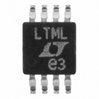
LT1962EMS8-3.3#TR Linear Technology, LT1962EMS8-3.3#TR Datasheet - Page 11

LT1962EMS8-3.3#TR
Manufacturer Part Number
LT1962EMS8-3.3#TR
Description
IC LDO REG LOWNOISE 3.3V 8-MSOP
Manufacturer
Linear Technology
Datasheet
1.LT1962EMS8PBF.pdf
(16 pages)
Specifications of LT1962EMS8-3.3#TR
Regulator Topology
Positive Fixed
Voltage - Output
3.3V
Voltage - Input
Up to 20V
Voltage - Dropout (typical)
0.27V @ 300mA
Number Of Regulators
1
Current - Output
300mA
Current - Limit (min)
320mA
Operating Temperature
-40°C ~ 125°C
Mounting Type
Surface Mount
Package / Case
8-MSOP, Micro8™, 8-uMAX, 8-uSOP,
Lead Free Status / RoHS Status
Contains lead / RoHS non-compliant
Other names
LT1962EMS8-3.3TR
Available stocks
Company
Part Number
Manufacturer
Quantity
Price
APPLICATIO S I FOR ATIO
PI FU CTIO S
pin. The ADJ pin voltage is 1.22V referenced to ground and
the output voltage range is 1.22V to 20V.
BYP (Pin 3): Bypass. The BYP pin is used to bypass the
reference of the LT1962 to achieve low noise performance
from the regulator. The BYP pin is clamped internally to
pin will bypass the reference to lower the output voltage
noise. A maximum value of 0.01 F can be used for
reducing output voltage noise to a typical 20 V
10Hz to 100kHz bandwidth. If not used, this pin must be
left unconnected.
GND (Pin 4): Ground.
SHDN (Pin 5): Shutdown. The SHDN pin is used to put the
LT1962 regulators into a low power shutdown state. The
output will be off when the SHDN pin is pulled low. The
The LT1962 series are 300mA low dropout regulators with
micropower quiescent current and shutdown. The devices
are capable of supplying 300mA at a dropout voltage of
300mV. Output voltage noise can be lowered to 20 V
over a 10Hz to 100kHz bandwidth with the addition of a
0.01 F reference bypass capacitor. Additionally, the refer-
ence bypass capacitor will improve transient response of
the regulator, lowering the settling time for transient load
conditions. The low operating quiescent current (30 A)
drops to less than 1 A in shutdown. In addition to the low
quiescent current, the LT1962 regulators incorporate sev-
eral protection features which make them ideal for use in
battery-powered systems. The devices are protected
against both reverse input and reverse output voltages. In
battery backup applications where the output can be held
0.6V (one V
U
V
IN
U
+
BE
Figure 1. Kelvin Sense Connection
). A small capacitor from the output to this
8
5
U
U
IN
SHDN
LT1962
GND
U
4
SENSE
OUT
1
2
W
R
R
P
P
+
1962 F01
LOAD
RMS
U
over a
RMS
SHDN pin can be driven either by 5V logic or open-
collector logic with a pull-up resistor. The pull-up resistor
is required to supply the pull-up current of the open-
collector gate, normally several microamperes, and the
SHDN pin current, typically 1 A. If unused, the SHDN pin
must be connected to V
the SHDN pin is not connected.
NC (Pins 6, 7): No Connect. These pins are not internally
connected. For improved power handling capabilities,
these pins can be connected to the PC board.
IN (Pin 8): Input. Power is supplied to the device through
the IN pin. A bypass capacitor is required on this pin if the
device is more than six inches away from the main input
filter capacitor. In general, the output impedance of a
battery rises with frequency, so it is advisable to include a
bypass capacitor in battery-powered circuits. A bypass
capacitor in the range of 1 F to 10 F is sufficient. The
LT1962 regulators are designed to withstand reverse
voltages on the IN pin with respect to ground and the OUT
pin. In the case of a reverse input, which can happen if a
battery is plugged in backwards, the device will act as if
there is a diode in series with its input. There will be no
reverse current flow into the regulator and no reverse
voltage will appear at the load. The device will protect both
itself and the load.
up by a backup battery when the input is pulled to ground,
the LT1962-X acts like it has a diode in series with its
output and prevents reverse current flow. Additionally, in
dual supply applications where the regulator load is re-
turned to a negative supply, the output can be pulled below
ground by as much as 20V and still allow the device to start
and operate.
Adjustable Operation
The adjustable version of the LT1962 has an output
voltage range of 1.22V to 20V. The output voltage is set by
the ratio of two external resistors as shown in Figure 2. The
device servos the output to maintain the ADJ pin voltage
at 1.22V referenced to ground. The current in R1 is then
equal to 1.22V/R1 and the current in R2 is the current in R1
IN
. The device will not function if
LT1962 Series
11


