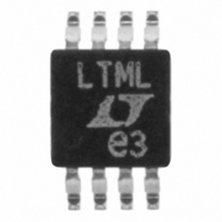
LT1962EMS8#TRPBF Linear Technology, LT1962EMS8#TRPBF Datasheet - Page 4

LT1962EMS8#TRPBF
Manufacturer Part Number
LT1962EMS8#TRPBF
Description
IC LDO REG LOWNOISE ADJ 8-MSOP
Manufacturer
Linear Technology
Datasheet
1.LT1962EMS8PBF.pdf
(16 pages)
Specifications of LT1962EMS8#TRPBF
Regulator Topology
Positive Adjustable
Voltage - Output
1.22 ~ 20 V
Voltage - Input
1.8 ~ 20 V
Voltage - Dropout (typical)
0.27V @ 300mA
Number Of Regulators
1
Current - Output
300mA
Current - Limit (min)
320mA
Operating Temperature
-40°C ~ 125°C
Mounting Type
Surface Mount
Package / Case
8-MSOP, Micro8™, 8-uMAX, 8-uSOP,
Lead Free Status / RoHS Status
Lead free / RoHS Compliant
Available stocks
Company
Part Number
Manufacturer
Quantity
Price
LT1962 Series
Note 5: Operating conditions are limited by maximum junction
temperature. The regulated output voltage specification will not apply for
all possible combinations of input voltage and output current. When
operating at maximum input voltage, the output current range must be
limited. When operating at maximum output current, the input voltage
range must be limited.
Note 6: To satisfy requirements for minimum input voltage, the LT1962
(adjustable version) is tested and specified for these conditions with an
external resistor divider (two 250k resistors) for an output voltage of
2.44V. The external resistor divider will add a 5 A DC load on the output.
Note 7: Dropout voltage is the minimum input to output voltage differential
needed to maintain regulation at a specified output current. In dropout, the
output voltage will be equal to: V
Note 8: GND pin current is tested with V
(whichever is greater) and a current source load. This means the device is
ELECTRICAL CHARACTERISTICS
TYPICAL PERFOR A CE CHARACTERISTICS
4
400
350
300
250
200
150
100
50
45
40
35
30
25
20
15
10
50
5
0
0
–50
0
Typical Dropout Voltage
Quiescent Current
V
V
R
/2.5/-3/-3.3/-5)
R
IN
SHDN
L
L
=
= 250k, I
–25
= 6V
50
= V
, I
L
IN
OUTPUT CURRENT (mA)
= 0 (LT1962-1.5/-1.8
0
L
TEMPERATURE ( C)
100
= 5 A (LT1962)
T
T
25
J
J
= 125 C
= 25 C
150
50
200
IN
75
– V
W
DROPOUT
250
100
IN
1962 G04
1962 G01
= V
U
125
300
OUT(NOMINAL)
.
1.532
1.524
1.516
1.508
1.500
1.492
1.484
1.476
1.468
500
450
400
350
300
250
200
150
100
50
0
or V
–50
0
Guaranteed Dropout Voltage
LT1962-1.5 Output Voltage
I
L
IN
= TEST POINTS
= 1mA
–25
= 2.3V
50
OUTPUT CURRENT (mA)
0
TEMPERATURE ( C)
100
25
150
tested while operating in its dropout region. This is the worst-case GND
pin current. The GND pin current will decrease slightly at higher input
voltages.
Note 9: ADJ pin bias current flows into the ADJ pin.
Note 10: SHDN pin current flows into the SHDN pin. This current is
included in the specification for GND pin current.
Note 11: Reverse output current is tested with the IN pin grounded and the
OUT pin forced to the rated output voltage. This current flows into the OUT
pin and out the GND pin.
Note 12: For the LT1962, LT1962-1.5 and LT1962-1.8 dropout voltage will
be limited by the minimum input voltage specification under some output
voltage/load conditions. See the curve of Minimum Input Voltage in the
Typical Performance Characteristics. For other fixed voltage versions of
the LT1962, the minimum input voltage is limited by the dropout voltage.
50
T
T
J
J
200
125 C
25 C
75
250
100
1962 G05
1962 G02
125
300
1.836
1.827
1.818
1.809
1.800
1.791
1.782
1.773
1.764
400
350
300
250
200
150
100
50
0
– 50
–50
Dropout Voltage
LT1962-1.8 Output Voltage
I
L
= 1mA
– 25
–25
0
0
TEMPERATURE ( C)
TEMPERATURE ( C)
I
L
I
= 10mA
L
I
25
L
25
= 100mA
= 300mA
50
50
I
L
= 1mA
75
75
I
L
= 50mA
100
100
1962 G06
1962 G03
125
125


