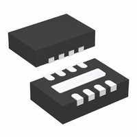
LT3080EDD-1#TRPBF Linear Technology, LT3080EDD-1#TRPBF Datasheet - Page 9

LT3080EDD-1#TRPBF
Manufacturer Part Number
LT3080EDD-1#TRPBF
Description
IC REG LDO ADJ 1.1A 8-DFN
Manufacturer
Linear Technology
Datasheet
1.LT3080EDD-1PBF.pdf
(24 pages)
Specifications of LT3080EDD-1#TRPBF
Regulator Topology
Positive Adjustable
Voltage - Output
0 ~ 36 V
Voltage - Input
1.2 ~ 36 V
Voltage - Dropout (typical)
1.35V @ 1.1A
Number Of Regulators
1
Current - Output
1.1A
Current - Limit (min)
1.1A
Operating Temperature
-40°C ~ 125°C
Mounting Type
Surface Mount
Package / Case
8-DFN
Lead Free Status / RoHS Status
Lead free / RoHS Compliant
Available stocks
Company
Part Number
Manufacturer
Quantity
Price
APPLICATIONS INFORMATION
dissipation: a higher voltage supply for the control circuitry
and a lower voltage supply for the collector. This increases
effi ciency and reduces dissipation. To further spread the
heat, a resistor can be inserted in series with the collector
to move some of the heat out of the IC and spread it on
the PC board.
The LT3080-1 can be operated in two modes. Three terminal
mode has the control pin connected to the power input pin
which gives a limitation of 1.35V dropout. Alternatively,
the “control” pin can be tied to a higher voltage and the
power IN pin to a lower voltage giving 300mV dropout
on the IN pin and minimizing the power dissipation. This
allows for a 1.1A supply regulating from 2.5V
or 1.8V
Output Voltage
The LT3080-1 generates a 10μA reference current that
fl ows out of the SET pin. Connecting a resistor from SET
to ground generates a voltage that becomes the reference
point for the error amplifi er (see Figure 1). The reference
voltage is a straight multiplication of the SET pin current
and the value of the resistor. Any voltage can be generated
and there is no minimum output voltage for the regulator.
A minimum load current of 1mA is required to maintain
regulation regardless of output voltage. For true zero voltage
output operation, this 1mA load current must be returned
to a negative supply voltage.
With the low level current used to generate the reference
voltage, leakage paths to or from the SET pin can create
errors in the reference and output voltages. High quality
insulation should be used (e.g., Tefl on, Kel-F); cleaning
+
IN
V
IN
to 1.2V
+
Figure 1. Basic Adjustable Regulator
V
V
CONTROL
CONTROL
OUT
IN
with low dissipation.
SET
R
SET
+
–
LT3080-1
C
SET
25mΩ
30801 F01
OUT
IN
to 1.8V
V
C
OUT
OUT
OUT
of all insulating surfaces to remove fl uxes and other
residues will probably be required. Surface coating may be
necessary to provide a moisture barrier in high humidity
environments.
Board leakage can be minimized by encircling the SET
pin and circuitry with a guard ring operated at a potential
close to itself; the guard ring should be tied to the OUT
pin. Guarding both sides of the circuit board is required.
Bulk leakage reduction depends on the guard ring width.
Ten nanoamperes of leakage into or out of the SET pin and
associated circuitry creates a 0.1% error in the reference
voltage. Leakages of this magnitude, coupled with other
sources of leakage, can cause signifi cant offset voltage
and reference drift, especially over the possible operating
temperature range.
If guardring techniques are used, this bootstraps any
stray capacitance at the SET pin. Since the SET pin is
a high impedance node, unwanted signals may couple
into the SET pin and cause erratic behavior. This will
be most noticeable when operating with minimum
output capacitors at full load current. The easiest way
to remedy this is to bypass the SET pin with a small
amount of capacitance from SET to ground, 10pF to
20pF is suffi cient.
Stability and Output Capacitance
The LT3080-1 requires an output capacitor for stability.
It is designed to be stable with most low ESR capacitors
(typically ceramic, tantalum or low ESR electrolytic). A
minimum output capacitor of 2.2μF with an ESR of 0.5Ω
or less is recommended to prevent oscillations. Larger
values of output capacitance decrease peak deviations
and provide improved transient response for larger load
current changes. Bypass capacitors, used to decouple
individual components powered by the LT3080-1, increase
the effective output capacitor value.
For improvement in transient performance, place a
capacitor across the voltage setting resistor. Capacitors
up to 1μF can be used. This bypass capacitor reduces
system noise as well, but start-up time is proportional
to the time constant of the voltage setting resistor (R
in Figure 1) and SET pin bypass capacitor.
LT3080-1
30801fa
9
SET


