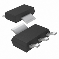
LT1129IST-5#TRPBF Linear Technology, LT1129IST-5#TRPBF Datasheet - Page 9

LT1129IST-5#TRPBF
Manufacturer Part Number
LT1129IST-5#TRPBF
Description
IC LDO REG W/SD 5V SOT223-3
Manufacturer
Linear Technology
Datasheet
1.LT1129CTPBF.pdf
(16 pages)
Specifications of LT1129IST-5#TRPBF
Regulator Topology
Positive Fixed
Voltage - Output
5V
Voltage - Input
Up to 30V
Voltage - Dropout (typical)
0.45V @ 700mA
Number Of Regulators
1
Current - Output
700mA
Operating Temperature
-40°C ~ 125°C
Mounting Type
Surface Mount
Package / Case
SOT-223 (3 leads + Tab), SC-73, TO-261
Lead Free Status / RoHS Status
Lead free / RoHS Compliant
Current - Limit (min)
-
Available stocks
Company
Part Number
Manufacturer
Quantity
Price
The LT1129 is a micropower low dropout regulator with
shutdown, capable of supplying 700mA of output current
at a dropout voltage of 0.4V. The device operates with very
low quiescent current (50μA). In shutdown the quiescent
current drops to only 16μA. In addition to the low quies-
cent current the LT1129 incorporates several protection
PIN FUNCTIONS
Input Pin: Power is supplied to the device through the
input pin. The input pin should be bypassed to ground
if the device is more than 6 inches away from the main
input fi lter capacitor. In general, the output impedance of
a battery rises with frequency so it is advisable to include
a bypass capacitor in battery-powered circuits. A bypass
capacitor in the range of 1μF to 10μF is suffi cient. The
LT1129 is designed to withstand reverse voltages on the
input pin with respect to both ground and the output pin.
In the case of a reversed input, which can happen if a
battery is plugged in backwards, the LT1129 will act as if
there is a diode in series with its input. There will be no
reverse current fl ow into the LT1129 and no reverse volt-
age will appear at the load. The device will protect both
itself and the load.
Output Pin: The output pin supplies power to the load. An
output capacitor is required to prevent oscillations. See
the Applications Information section for recommended
value of output capacitance and information on reverse
output characteristics.
Shutdown Pin (SHDN): This pin is used to put the device
into shutdown. In shutdown the output of the device is
turned off. This pin is active low. The device will be shut
down if the shutdown pin is actively pulled low. The
shutdown pin current with the pin pulled to ground will
be 6μA. The shutdown pin is internally clamped to 7V
and – 0.6V (one V
driven directly by 5V logic or by open collector logic with
a pull-up resistor. The pull-up resistor is only required
to supply the leakage current of the open collector gate,
normally several microamperes. Pull-up current must be
limited to a maximum of 20mA. A curve of shutdown pin
input current as a function of voltage appears in the Typical
Performance Characteristics. If the shutdown pin is not
APPLICATIONS INFORMATION
BE
). This allows the shutdown pin to be
used it can be left open circuit. The device will be active,
output on, if the shutdown pin is not connected.
Sense Pin: For fi xed voltage versions of the LT1129
(LT1129-3.3, LT1129-5) the sense pin is the input to the
error amplifi er. Optimum regulation will be obtained at the
point where the sense pin is connected to the output pin.
For most applications the sense pin is connected directly
to the output pin at the regulator. In critical applications
small voltage drops caused by the resistance (R
traces between the regulator and the load, which would
normally degrade regulation, may be eliminated by con-
necting the sense pin to the output pin at the load as
shown in Figure 1 (Kelvin Sense Connection). Note that
the voltage drop across the external PC traces will add to
the dropout voltage of the regulator. The sense pin bias
current is 15μA at the nominal regulated output voltage.
This pin is internally clamped to –0.6V (one V
Adjust Pin: For the LT1129 (adjustable version) the adjust
pin is the input to the error amplifi er. This pin is internally
clamped to 6V and –0.6V (one V
current of 150nA which fl ows into the pin. See Bias Cur-
rent curve in the Typical Performance Characteristics. The
adjust pin reference voltage is equal to 3.75V referenced
to ground.
features which make it ideal for use in battery-powered
systems. The device is protected against reverse input
voltages. In battery backup applications where the output
can be held up by a backup battery when the input is pulled
to ground, the LT1129 acts like it has a diode in series
with its output and prevents reverse current fl ow.
LT1129/LT1129-3.3/LT1129-5
1μF
Figure 1. Kelvin Sense Connection
SHDN
IN
LT1129
GND
SENSE
OUT
R
R
10μF
BE
P
P
). This pin has a bias
+
LOAD
112935 F01
BE
).
P
) of PC
112935ff
9


