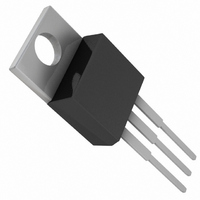
LT1585ACT-1.5 Linear Technology, LT1585ACT-1.5 Datasheet - Page 2

LT1585ACT-1.5
Manufacturer Part Number
LT1585ACT-1.5
Description
IC LDO REG 5A 1.5V TO220-3
Manufacturer
Linear Technology
Datasheet
1.LT1585ACT-1.5.pdf
(8 pages)
Specifications of LT1585ACT-1.5
Regulator Topology
Positive Fixed
Voltage - Output
1.5V
Voltage - Input
Up to 7V
Voltage - Dropout (typical)
1.2V @ 5A
Number Of Regulators
1
Current - Limit (min)
5A
Operating Temperature
0°C ~ 125°C
Mounting Type
Through Hole
Package / Case
TO-220-3 (Straight Leads)
Lead Free Status / RoHS Status
Contains lead / RoHS non-compliant
Current - Output
-
Available stocks
Company
Part Number
Manufacturer
Quantity
Price
Part Number:
LT1585ACT-1.5
Manufacturer:
LT/凌特
Quantity:
20 000
ABSOLUTE
PACKAGE/ORDER
LT1585-1.5/LT1585A-1.5
V
Operating Junction Temperature Range
Consult factory for Industrial and Military grade parts.
temperature range, otherwise specifications are at T
PARAMETER
Output Voltage (Note 4)
Line Regulation (Notes 2, 3)
Load Regulation
(Notes 2, 3, 4)
Dropout Voltage (Note 4)
Current Limit
Quiescent Current
Ripple Rejection (Note 4)
Thermal Regulation
Temperature Stability
Long-Term Stability
RMS Output Noise
(% of V
Thermal Resistance
Junction to Case
Note 1: Absolute Maximum Ratings are those values beyond which the life
of the device may be impaired.
Note 2: See thermal regulation specifications for changes in output voltage
due to heating effects. Load and line regulation are measured at a constant
junction temperature by low duty cycle pulse testing.
Note 3: Line and load regulation are guaranteed up to the maximum
power dissipation (25W for the LT1585-1.5 in T package and 27.5W for
2
ELECTRICAL CHARACTERISTICS
OUTPUT
IN
............................................................................ 7V
TAB
Control Section .................................. 0 C to 125 C
Power Transistor ................................ 0 C to 150 C
IS
OUT
)
3-LEAD PLASTIC DD
FRONT VIEW
JA
M PACKAGE
= 30 C/W*
3
2
1
W
MAXIMUM
V
V
GND
IN
OUT
W W
*WITH PACKAGE
SOLDERED TO 0.5
SQUARE INCH COPPER
AREA OVER BACKSIDE
GROUND PLANE OR
INTERNAL POWER PLANE.
20 C/W TO > 40 C/W
WITH OTHER MOUNTING
TECHNIQUES
CONDITIONS
V
3V V
3V V
V
LT1585-1.5, (V
LT1585A-1.5, (V
V
f = 120Hz, C
T
T
T
T Package: Control Circuitry/Power Transistor
M Package: Control Circuitry/Power Transistor
JA
A
A
A
IN
IN
V
IN
CAN VARY FROM
OUT
= 25 C, 30ms Pulse
= 125 C, 1000 Hrs.
= 25 C, 10Hz f 10kHz
= 5V
INFORMATION
= 5V, T
= 5V, T
U
IN
IN
= 1%, I
J
J
7V, 0mA I
7V, I
RATINGS
= 25 C, I
OUT
= 25 C, 0mA I
OUT
IN
OUT
= 25 F Tant., V
IN
– V
W
= I
– V
= 0mA
OUT
FULL LOAD
OUT
U
OUT
OUT
LT1585CM-1.5
LT1585ACM-1.5
A
) = 5.5V
= 0mA
ORDER PART
= 25 C.
) = 5.5V
NUMBER
OUT
I
FULL LOAD
The
IN
U
(Note 1)
= 4.5V, I
I
FULL LOAD
denotes specifications which apply over the specified operating
OUT
PRECONDITIONI G
Storage Temperature Range ................ – 65 C to 150 C
Lead Temperature (Soldering, 10 sec)................. 300 C
100% Thermal Limit Functional Test
the LT1585A-1.5). Power dissipation is determined by input/output
differential and the output current. Guaranteed maximum output power
will not be available over the full input/output voltage range.
Note 4: I
as a function of input-to-output voltage. I
LT1585-1.5 and 5A for the LT1585A-1.5. The LT1585-1.5/LT1585A-1.5
have constant current limit with changes in input-to-output voltage.
= I
OUTPUT
FULL LOAD
TAB IS
FULL LOAD
3-LEAD PLASTIC TO-220
U
FRONT VIEW
is defined as the maximum value of output load current
JA
T PACKAGE
= 50 C/W
1.485 (– 1%)
1.470 (– 2%)
3
2
1
4.60
5.00
MIN
U U
60
FULL LOAD
0.005
1.200
0.004
0.003
0.05
0.05
5.25
6.00
0.03
TYP
1.5
1.5
0.5
72
7
V
V
GND
IN
OUT
is equal to 4.6A for the
1.515 (+ 1%)
1.530 (+ 2%)
LT1585CT-1.5
LT1585ACT-1.5
0.7/3.0
0.7/3.0
ORDER PART
1.400
MAX
0.02
0.2
0.3
0.5
1.0
13
NUMBER
UNITS
%/W
C/W
C/W
mA
dB
%
%
%
%
%
%
V
V
V
A
A


