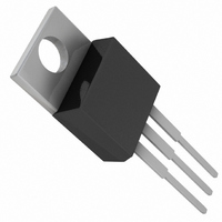
LT1585ACT-3.3 Linear Technology, LT1585ACT-3.3 Datasheet - Page 7

LT1585ACT-3.3
Manufacturer Part Number
LT1585ACT-3.3
Description
IC LDO REG 5A 3.3V TO220-3
Manufacturer
Linear Technology
Datasheet
1.LT1585ACT-3.3PBF.pdf
(12 pages)
Specifications of LT1585ACT-3.3
Regulator Topology
Positive Fixed
Voltage - Output
3.3V
Voltage - Input
Up to 7V
Voltage - Dropout (typical)
1.2V @ 5A
Number Of Regulators
1
Current - Limit (min)
5A
Operating Temperature
0°C ~ 125°C
Mounting Type
Through Hole
Package / Case
TO-220-3 (Straight Leads)
Lead Free Status / RoHS Status
Contains lead / RoHS non-compliant
Current - Output
-
Available stocks
Company
Part Number
Manufacturer
Quantity
Price
Company:
Part Number:
LT1585ACT-3.3
Manufacturer:
LT
Quantity:
5 510
Part Number:
LT1585ACT-3.3
Manufacturer:
LT/凌特
Quantity:
20 000
Part Number:
LT1585ACT-3.3#PBF
Manufacturer:
LINEAR/凌特
Quantity:
20 000
APPLICATIONS
A protection diode between the input and output pins is
usually not needed. An internal diode between the input
and output pins on the LT1585A/LT1585A-3.3 can handle
microsecond surge currents of 50A to 100A. Even with
large value output capacitors it is difficult to obtain those
values of surge currents in normal operation. Only with
large values of output capacitance, such as 1000µF to
5000µF, and with the input pin instantaneously shorted to
ground can damage occur. A crowbar circuit at the input
of the LT1585A/LT1585A-3.3 can generate those levels of
current, and a diode from output to input is then recom-
mended. This is shown in Figure 2. Usually, normal power
supply cycling or system “hot plugging and unplugging”
will not generate current large enough to do any damage.
The adjust pin can be driven on a transient basis ±7V with
respect to the output, without any device degradation. As
with any IC regulator, exceeding the maximum input-to-
output voltage differential causes the internal transistors
to break down and none of the protection circuitry is then
functional.
V
V
IN
IN
+
+
C1
10µF
C1
10µF
U
IN
IN
LT1585A-3.3
(OPTIONAL)
(OPTIONAL)
LT1585A
1N4002
1N4002
+
GND
ADJ
D1
D1
INFORMATION
Figure 2
U
C
OUT
OUT
ADJ
W
+
R1
R2
C2
100µF
+
V
OUT
LT1585A • F02
U
C2
100µF
V
OUT
Ripple Rejection
The typical curve for ripple rejection reflects values for the
LT1585A-3.3 fixed output voltage part. In applications
that require improved ripple rejection, use the adjustable
device. A bypass capacitor from the adjust pin to ground
reduces the output ripple by the ratio of V
impedance of the adjust pin capacitor at the ripple fre-
quency should be less than the value of R1 (typically in the
range of 100Ω to 120Ω) in the feedback divider network
in Figure 2. Therefore, the value of the required adjust pin
capacitor is a function of the input ripple frequency. For
example, if R1 equals 100Ω and the ripple frequency
equals 120Hz, the adjust pin capacitor should be 22µF. At
10kHz, only 0.22µF is needed.
Output Voltage
The LT1585A adjustable regulator develops a 1.25V ref-
erence voltage between the output pin and the adjust pin
(see Figure 3). Placing a resistor R1 between these two
terminals causes a constant current to flow through R1
and down through R2 to set the overall output voltage.
Normally, this current is the specified minimum load
current of 10mA. The current out of the adjust pin adds to
the current from R1 and is typically 55µA. Its output
voltage contribution is small and only needs consider-
ation when very precise output voltage setting is required.
V
IN
V
OUT
+
= V
REF
Figure 3. Basic Adjustable Regulator
C1
10µF
(1 + R2/R1) + I
LT1585A/LT1585A-3.3
IN
55µA
I
ADJ
LT1585A
ADJ
ADJ
(R2)
OUT
V
REF
R1
R2
OUT
+
/1.25V. The
C2
100µF
LT1585A • F03
V
OUT
1585afa
7


