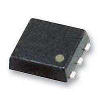
S-1167B30-I6T2G Seiko Instruments, S-1167B30-I6T2G Datasheet - Page 13

S-1167B30-I6T2G
Manufacturer Part Number
S-1167B30-I6T2G
Description
IC REG LDO 150MA 3.0V SNT-6A
Manufacturer
Seiko Instruments
Datasheet
1.S-1167B15-M5T1G.pdf
(31 pages)
Specifications of S-1167B30-I6T2G
Regulator Topology
Positive Fixed
Voltage - Output
3V
Voltage - Input
Up to 6.5V
Voltage - Dropout (typical)
0.15V @ 100mA
Number Of Regulators
1
Current - Output
150mA (Min)
Operating Temperature
-40°C ~ 85°C
Mounting Type
Surface Mount
Package / Case
SNT-6A
Number Of Outputs
1
Polarity
Positive
Input Voltage Max
6.5 V
Output Voltage
3 V
Output Type
Fixed
Dropout Voltage (max)
0.23 V at 100 mA
Output Current
150 mA
Line Regulation
0.2 % / V
Load Regulation
40 mV
Voltage Regulation Accuracy
1 %
Maximum Power Dissipation
0.5 W
Maximum Operating Temperature
+ 85 C
Mounting Style
SMD/SMT
Minimum Operating Temperature
- 40 C
Lead Free Status / RoHS Status
Lead free / RoHS Compliant
Current - Limit (min)
-
Lead Free Status / Rohs Status
Details
Rev.3.0
Operation
1. Basic Operation
2. Output Transistor
ULTRA LOW CURRENT CONSUMPTION, HIGH RIPPLE REJECTION AND LOW DROPOUT CMOS VOLTAGE REGULATOR
Figure 12 shows the block diagram of the S-1167 Series.
The error amplifier compares the reference voltage (V
feedback resistors R
output voltage free of any fluctuations of input voltage and temperature.
The S-1167 Series uses a low on-resistance P-channel MOS FET as the output transistor.
Be sure that V
current flowing from the VOUT pin through a parasitic diode to the VIN pin.
_00
OUT
Current supply
*1. Parasitic diode
does not exceed V
VIN
VSS
s
and R
Reference voltage
V
f
. It supplies the output transistor with the gate voltage necessary to ensure a certain
ref
circuit
IN
+ 0.3 V to prevent the voltage regulator from being damaged due to inverse
Error amplifier
Seiko Instruments Inc.
−
+
Figure 12
ref
) with V
fb
, which is the output voltage resistance-divided by
V
R
R
fb
f
s
*1
S-1167 Series
VOUT
13


