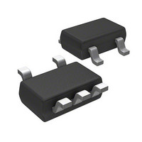
MIC5253-2.8BC5 Micrel Inc, MIC5253-2.8BC5 Datasheet - Page 7

MIC5253-2.8BC5
Manufacturer Part Number
MIC5253-2.8BC5
Description
IC REG LDO 100MA 2.8V SC70-5
Manufacturer
Micrel Inc
Series
Teeny™r
Datasheet
1.MIC5253-3.3YC5_TR.pdf
(9 pages)
Specifications of MIC5253-2.8BC5
Regulator Topology
Positive Fixed
Voltage - Output
2.8V
Voltage - Input
Up to 5.5V
Voltage - Dropout (typical)
0.165V @ 100mA
Number Of Regulators
1
Current - Output
100mA
Current - Limit (min)
150mA
Operating Temperature
-40°C ~ 125°C
Mounting Type
Surface Mount
Package / Case
SC-70-5, SC-88A, SOT-323-5, SOT-353, 5-TSSOP
Lead Free Status / RoHS Status
Contains lead / RoHS non-compliant
Available stocks
Company
Part Number
Manufacturer
Quantity
Price
Company:
Part Number:
MIC5253-2.8BC5
Manufacturer:
MICREL
Quantity:
38 000
November 2005
Applications Information
Enable/Shutdown
The MIC5253 comes with an active-high enable pin that
allows the regulator to be disabled. Forcing the enable pin low
disables the regulator and sends it into a “zero” off-mode-
current state. In this state, current consumed by the regulator
goes nearly to zero. Forcing the enable pin high enables the
output voltage. This part is CMOS and the enable pin cannot
be left floating; a floating enable pin may cause an indetermi-
nate state on the output.
Input Capacitor
The MIC5253 is a high performance, high bandwidth device.
Therefore, it requires a well-bypassed input supply for opti-
mal performance. A 1 F capacitor is required from the input
to ground to provide stability. Low-ESR ceramic capacitors
provide optimal performance at a minimum of space. Addi-
tional high-frequency capacitors, such as small valued NPO
dielectric type capacitors, help filter out high frequency noise
and are good practice in any RF based circuit.
Output Capacitor
The MIC5253 requires an output capacitor for stability. The
design requires 1 F or greater on the output to maintain
stability. The design is optimized for use with low-ESR
ceramic chip capacitors. High ESR capacitors may cause
high frequency oscillation. The maximum recommended
ESR is 300m . The output capacitor can be increased, but
performance has been optimized for a 1 F ceramic output
capacitor and does not improve significantly with larger
capacitance.
X7R/X5R dielectric-type ceramic capacitors are recom-
mended because of their temperature performance. X7R-
type capacitors change capacitance by 15% over their oper-
ating temperature range and are the most stable type of
ceramic capacitors. Z5U and Y5V dielectric capacitors change
value by as much as 50% and 60%, respectively, over their
operating temperature ranges. To use a ceramic chip capaci-
tor with Y5V dielectric, the value must be much higher than an
X7R ceramic capacitor to ensure the same minimum capaci-
tance over the equivalent operating temperature range.
Bypass Capacitor
A capacitor can be placed from the noise bypass pin to
ground to reduce output voltage noise. The capacitor by-
passes the internal reference. A 0.01 F capacitor is recom-
mended for applications that require low-noise outputs. The
bypass capacitor can be increased, further reducing noise
and improving PSRR. Turn-on time increases slightly with
respect to bypass capacitance. A unique quick-start circuit
allows the MIC5253 to drive a large capacitor on the bypass
pin without significantly slowing turn-on time. Refer to the
“Typical Characteristics” section for performance with differ-
ent bypass capacitors.
Active Shutdown
The MIC5253 also features an active shutdown clamp, which
is an N-channel MOSFET that turns on when the device is
disabled. This allows the output capacitor and load to dis-
charge, de-energizing the load.
MIC5253
7
No-Load Stability
The MIC5253 will remain stable and in regulation with no load
unlike many other voltage regulators. This is especially
important in CMOS RAM keep-alive applications.
Thermal Considerations
The MIC5253 is designed to provide 100mA of continuous
current in a very small package. Maximum ambient operating
temperature can be calculated based on the output current
and the voltage drop across the part. Given that the input
voltage is 5.0V, the output voltage is 2.9V, and the output
current = 100mA.
The actual power dissipation of the regulator circuit can be
determined using the equation:
Because this device is CMOS and the ground current is
typically <100 A over the load range, the power dissipation
contributed by the ground current is < 1% and can be ignored
for this calculation.
To determine the maximum ambient operating temperature
of the package, use the junction-to-ambient thermal resis-
tance of the device and the following basic equation:
Table 1 shows junction-to-ambient thermal resistance for the
MIC5253 in the SC-70 package.
Substituting P
operating temperature will give the maximum operating con-
ditions for the regulator circuit. The junction-to-ambient ther-
mal resistance for the minimum footprint is 400 C/W, from
Table 1. The maximum power dissipation must not be ex-
ceeded for proper operation.
For example, when operating the MIC5253-2.9BC5 at an
input voltage of 5.0V and 100mA load with a minimum
footprint layout, the maximum ambient operating tempera-
ture T
SC-70-5 (C5)
Package
P
P
P
T
P (max)
A
0.21W
T
JA
J
D
D
D
D
A
(max) = 125 C, the max. junction temperture of the die
can be determined as follows:
= (V
= (5.0V – 2.9V)
= 0.21W
thermal resistance = 400 C/W
41
IN
C
125 C T
Table 1. Thermal Resistance
D
400
– V
Minimum Footprint
for P
JA
T (max) T
OUT
J
C/W
Recommended
400 C/W
D
A
) I
(max) and solving for the ambient
JA
OUT
100mA
A
+ V
IN
I
GND
Copper Clad
JA
325 C
1" Sq.
M9999-112305
250 C/W
Micrel
JC


