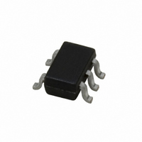
LP5951MGX-2.8/NOPB National Semiconductor, LP5951MGX-2.8/NOPB Datasheet

LP5951MGX-2.8/NOPB
Specifications of LP5951MGX-2.8/NOPB
Related parts for LP5951MGX-2.8/NOPB
LP5951MGX-2.8/NOPB Summary of contents
Page 1
... The device is available in SOT23-5 and SC70-5 package. The device is available in fixed output voltages in the range of 1.3V to 3.7V. For availability, please contact your local NSC sales office. Typical Application Circuit © 2011 National Semiconductor Corporation LP5951 Features ■ Excellent line transient response: ±2mV typ. ...
Page 2
Connection Diagrams 5-Lead Small Outline Package SOT23-5 (MF) Top View See NS Package Number MF05A Pin Descriptions Pin Number Pin Name Description 1 V Input Voltage. Input range: 1. GND Ground 3 EN Enable pin logic ...
Page 3
... Z: 1 Digit Assembly Plant Code, LP5951 Supplied as 3000 Units, Tape and Reel LP5951MGX-1.3 LP5951MGX-1.3 LP5951MGX-1.5 LP5951MGX-1.5 LP5951MGX-1.8 LP5951MGX-1.8 LP5951MGX-2.0 LP5951MGX-2.0 LP5951MGX-2.5 LP5951MGX-2.5 LP5951MGX-2.8 LP5951MGX-2.8 LP5951MGX-3.0 LP5951MGX-3.0 LP5951MGX-3.3 LP5951MGX-3.3 LP5951MGX-3.7 LP5951MGX-3 Digit Date Code, TT: 2 Digit Dierun Code 3 Flow Package Marking L23 NOPB L23 ...
Page 4
... Human Body Model: Machine Model ESD Caution Notice National Semiconductor recommends that all integrated circuits be handled with appropriate precautions. Failure to observe proper ESD handling techniques can result in damage. Electrical Characteristics Typical values and limits appearing in standard typeface are for T operating temperature range: -40°C ...
Page 5
Enable Control Characteristics Symbol Parameter I Maximum Input Current Input EN V Low Input Threshold IL (shutdown) V High Input Threshold IH (enable) Transient Characteristics Symbol Parameter ΔV Dynamic Line V IN OUT Transient V OUT(NOM) ΔV ...
Page 6
Output Current Derating Maximum Load Current Block Diagram www.national.com , T = 85° 1.5V OUT A OUT 6 20136204 20136205 ...
Page 7
Typical Performance Characteristics ceramic 1V 25°C, Enable pin is tied OUT(NOM) A Load Transient Response Line Transient Response Enable Start-up Time Unless otherwise specified Load Transient Response 20136209 ...
Page 8
Output Voltage Change vs Temperature Power Supply Rejection Ratio www.national.com Ground Current vs V 20136217 20136215 8 IN 20136216 ...
Page 9
Application Hints POWER DISSIPATION AND DEVICE OPERATION The permissible power dissipation for any package is a mea- sure of the capability of the device to pass heat from the power source, the junctions of the IC, to the ultimate heat ...
Page 10
The ceramic capacitor’s capacitance can vary with tempera- ture. The capacitor type X7R, which operates over a temper- ature range of -55°C to +125°C, will only vary the capacitance to within ±15%. The capacitor type X5R has a similar toler- ...
Page 11
Physical Dimensions inches (millimeters) unless otherwise noted For most accurate revision please refer to www.national.com/packaging/parts/ NS Package Number MF05A 5-Lead Small Outline Package SOT23-5 (MF), NS Package Number MAA05A 5-Lead Small Outline Package SC70-5 (MG), 11 www.national.com ...
Page 12
... For more National Semiconductor product information and proven design tools, visit the following Web sites at: www.national.com Products Amplifiers www.national.com/amplifiers Audio www.national.com/audio Clock and Timing www.national.com/timing Data Converters www.national.com/adc Interface www.national.com/interface LVDS www.national.com/lvds Power Management www.national.com/power Switching Regulators www.national.com/switchers LDOs www.national.com/ldo LED Lighting www ...


