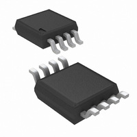
LP3981IMM-2.7/NOPB National Semiconductor, LP3981IMM-2.7/NOPB Datasheet - Page 8

LP3981IMM-2.7/NOPB
Manufacturer Part Number
LP3981IMM-2.7/NOPB
Description
IC REG LDO 300MA 2.7V 8MSOP
Manufacturer
National Semiconductor
Datasheet
1.LP3981IMM-3.3NOPB.pdf
(11 pages)
Specifications of LP3981IMM-2.7/NOPB
Regulator Topology
Positive Fixed
Voltage - Output
2.7V
Voltage - Input
Up to 6V
Voltage - Dropout (typical)
0.132V @ 300mA
Number Of Regulators
1
Current - Output
300mA
Current - Limit (min)
300mA
Operating Temperature
-40°C ~ 125°C
Mounting Type
Surface Mount
Package / Case
8-MSOP, Micro8™, 8-uMAX, 8-uSOP,
Lead Free Status / RoHS Status
Lead free / RoHS Compliant
Other names
LP3981IMM-2.7
LP3981IMM-2.7TR
LP3981IMM-2.7TR
www.national.com
Typical Performance Characteristics
C
Application Hints
POWER DISSIPATION AND DEVICE OPERATION
The permissible power dissipation for any package is a
measure of the capability of the device to pass heat from the
power source, the junctions of the IC, to the ultimate heat
sink, the ambient environment. Thus, the power dissipation
is dependant on the ambient temperature and the thermal
resistance across the various interfaces between the die and
ambient air.
BP
= 0.033 µF, V
(V
(V
IN
IN
Line Transient Response
Line Transient Response
= V
= V
Enable Response (T
IN
= V
OUT
OUT
OUT
+ 1V to V
+ 1V to V
+ 0.5V, T
OUT
OUT
A
ON
= 25˚C, Enable pin is tied to V
+ 1.6V)
+ 1.6V)
)
20020326
20020328
20020330
Unless otherwise specified, C
8
As stated in notes 3 and 5 in the electrical specifications
sections, the allowable power dissipation for the device in a
given package can be calculated using the equation:
With a θ
a value of 2.0W with a maximum junction temperature of
IN
. (Continued)
JA
= 50˚C/W, the device in theLLP package returns
(V
(V
IN
IN
Line Transient Response
Line Transient Response
= V
= V
Enable Response (T
OUT
OUT
+ 1V to V
+ 1V to V
IN
= C
OUT
OUT
OUT
= 2.2 µF Ceramic,
ON
+ 1.6V)
+ 1.6V)
)
20020327
20020329
20020331


