LP2960AIM-3.3/NOPB National Semiconductor, LP2960AIM-3.3/NOPB Datasheet - Page 12
LP2960AIM-3.3/NOPB
Manufacturer Part Number
LP2960AIM-3.3/NOPB
Description
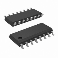
IC REG LDO 3.3V 500MA 16-SOIC
Manufacturer
National Semiconductor
Datasheet
1.LP2960IM-5.0NOPB.pdf
(16 pages)
Specifications of LP2960AIM-3.3/NOPB
Regulator Topology
Positive Fixed
Voltage - Output
3.3V
Voltage - Input
Up to 30V
Voltage - Dropout (typical)
0.47V @ 500mA
Number Of Regulators
1
Current - Output
500mA
Operating Temperature
-40°C ~ 125°C
Mounting Type
Surface Mount
Package / Case
16-SOIC (3.9mm Width)
Lead Free Status / RoHS Status
Lead free / RoHS Compliant
Current - Limit (min)
-
Other names
*LP2960AIM-3.3
*LP2960AIM-3.3/NOPB
LP2960AIM-3.3
*LP2960AIM-3.3/NOPB
LP2960AIM-3.3
Available stocks
Company
Part Number
Manufacturer
Quantity
Price
Company:

Part Number:
LP2960AIM-3.3/NOPB
Manufacturer:
NS
Quantity:
140


www.national.com
Application Hints
*
external supply. To avoid this invalid response, pull-up to regulator output.
**
The Error signal becomes low as V
goes high at about 5V input, where the output equals 4.75V.
Since the dropout voltage is load dependent, the input volt-
age trip points will vary with load current, but the output
voltage trip point does not.
The comparator has an open-collector output which requires
an external pull-up resistor. This resistor may be connected
to the LP2960 output or another supply voltage.
Best operation is obtained by connecting the pull-up to the
LP2960 output. If the pull-up resistor is connected to an
external 5V supply, the error flag will incorrectly signal
“HIGH” whenever V
Diagram).
In selecting a value for the pull-up resistor, note that while
the output can sink 400 µA, this current adds to battery drain.
Suggested values range from 100 kΩ–1 MΩ. The resistor is
not required if the output is unused.
If a large output capacitance is used, a false logic “HIGH”
can be generated when V
output becomes a high impedance, causing the voltage at
the error output to rise to its pull-up value. If the pull-up
resistor is connected to V
1.2V (which is a logic “HIGH” signal incorrectly signifying the
output is in regulation).
The user may wish to divide down the error flag voltage
using equal-value resistors (10 kΩ suggested) to ensure a
low-level logic signal during any fault condition, while still
allowing a valid high logic level during normal operation.
AUXILIARY COMPARATOR
The LP2960 contains an auxiliary comparator whose invert-
ing input is connected to the 1.23V reference. The auxiIiary
comparator has an open-collector output whose electrical
characteristics are similar to the dropout detection compara-
tor. The non-inverting input and output are brought out for
external connections.
SHUTDOWN INPUT
A logic-level signal will shut off the regulator output when a
“LOW” (
In shutdown mode, ERROR will go high if it has been pulled up to an
Exact value depends on dropout voltage. (See Application Hints)
<
1.2V) is applied to the Shutdown input.
Error Output Timing Diagram
IN
<
OUT
1.3V (see Error Output Timing
IN
≈1.3V. In this case, the error
, the error output can rise to
(Continued)
IN
exceeds about 1.3V. It
01196229
12
To prevent possible mis-operation, the Shutdown input must
be actively terminated. If the input is driven from open-
collector logic, a pull-up resistor (20 kΩ–100 kΩ recom-
mended) should be connected from the Shutdown input to
the regulator input.
If the Shutdown input is driven from a source which actively
pulls low and high (like an op-amp), the puIl-up resistor is not
required, but may be used.
If the Shutdown input is to be unused, the cost of the pull-up
resistor can be saved by tying the Shutdown input directly to
the regulator input.
IMPORTANT: Since the Absolute Maximum Ratings state
that the Shutdown input can not go more than 0.3V below
ground, the reverse-battery protection feature which protects
the regulator input is sacrificed if the Shutdown input is tied
directly to the regulator input.
If reverse-battery protection is required in an application, the
pull-up resistor between the Shutdown input and the regula-
tor input must be used.
GROUND CONNECTIONS
The pins designated GND (see Connection Diagrams) must
be connected to the high-current ground point in the circuit.
The GND pins are electrically connected (through the lead
frame) to the die substrate, making them ideal for conducting
ground current or heat (see Heatsinking).
The surface-mount (M) package also has an Analog Ground
pin, which is the ground point on the die for the regulator
reference circuitry.
Along with the Sense pin, the availability of the Analog
Ground pin allows the designer the ability to use “remote”
sensing and eliminate output voltage errors due to IR drops
occurring along PC board traces.
IMPORTANT: The Analog Ground pin must be connected to
circuit ground at some point for the regulator to operate.
If remote sensing is not needed, the Analog Ground pin can
simply be pin-strapped to the adjacent GND pin.
HEATSINKING
A heatsink may be required with the LP2960 depending on
the maximum power dissipation and maximum ambient tem-
perature of the application. Under alI possible operating
conditions, the junction temperature must be within the
range specified under Absolute Maximum Ratings.
To determine if a heatsink is required, the power dissipated
by the regulator, P
The figure below shows the voltages and currents which are
present in the circuit, as welI as the formula for calcuIating
the power dissipated in the regulator:
D
, must be calculated.
Related parts for LP2960AIM-3.3/NOPB
Image
Part Number
Description
Manufacturer
Datasheet
Request
R

Part Number:
Description:
Manufacturer:
National Semiconductor
Datasheet:
Part Number:
Description:
IC REG LDO 5V 500MA 16-SOIC
Manufacturer:
National Semiconductor
Datasheet:

Part Number:
Description:
IC REG LDO 5V 500MA 16-SOIC
Manufacturer:
National Semiconductor
Datasheet:
Part Number:
Description:
National Semiconductor [8-Bit D/A Converter]
Manufacturer:
National Semiconductor
Datasheet:
Part Number:
Description:
National Semiconductor [Media Coprocessor]
Manufacturer:
National Semiconductor
Datasheet:
Part Number:
Description:
Digitally Controlled Tone and Volume Circuit with Stereo Audio Power Amplifier, Microphone Preamp Stage and National 3D Sound
Manufacturer:
National Semiconductor
Datasheet:
Part Number:
Description:
Digitally Controlled Tone and Volume Circuit with Stereo Audio Power Amplifier, Microphone Preamp Stage and National 3D Sound
Manufacturer:
National Semiconductor
Datasheet:
Part Number:
Description:
AC97 Rev 2 Codec with Sample Rate Conversion and National 3D Sound
Manufacturer:
National Semiconductor
Part Number:
Description:
Manufacturer:
National Semiconductor
Datasheet:
Part Number:
Description:
Manufacturer:
National Semiconductor
Datasheet:
Part Number:
Description:
General Purpose, Low Voltage, Low Power, Rail-to-Rail Output Operational Amplifiers
Manufacturer:
National Semiconductor
Datasheet:
Part Number:
Description:
8-bit 20 MSPS flash A/D converter.
Manufacturer:
National Semiconductor
Datasheet:
Part Number:
Description:
Low Noise Quad Operational Amplifier
Manufacturer:
National Semiconductor
Datasheet:
Part Number:
Description:
Quad Differential Line Receivers
Manufacturer:
National Semiconductor
Datasheet: