LP38856T-0.8/NOPB National Semiconductor, LP38856T-0.8/NOPB Datasheet - Page 3
LP38856T-0.8/NOPB
Manufacturer Part Number
LP38856T-0.8/NOPB
Description
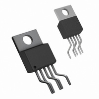
IC REG LDO 0.8V 3A TO220-5
Manufacturer
National Semiconductor
Series
PowerWise®r
Type
Voltage Regulatorr
Datasheet
1.LP38856T-0.8NOPB.pdf
(5 pages)
Specifications of LP38856T-0.8/NOPB
Package / Case
TO-220-5 (Bent and Staggered Leads)
Mounting Type
Through Hole
Current - Output
3A
Voltage - Output
0.8V
Voltage - Input
1.8 ~ 3 V
Operating Temperature
-40°C ~ 125°C
Regulator Topology
Positive Fixed
Voltage - Dropout (typical)
0.24V @ 3A
Number Of Regulators
1
Current, Output
3 A
Current, Supply
10 mA
Package Type
TO-220
Regulation, Line
0.04 %/V
Regulation, Load
0.2 %/A
Regulator Type
Linear, Low Dropout
Resistance, Thermal, Junction To Case
3 °C/W
Temperature, Operating, Range
-40 to +125 °C
Voltage, Dropout
240 mV
Voltage, Input
3 to 5.5 V
Voltage, Noise
150 μV
Voltage, Output
0.8 V
Voltage, Supply, Rejection Ratio
80 dB
Lead Free Status / RoHS Status
Lead free / RoHS Compliant
Current - Limit (min)
-
Lead Free Status / Rohs Status
RoHS Compliant part
Electrostatic Device
Other names
*LP38856T-0.8/NOPB::LP38856T-0.8


ΔV
ΔV
ΔV
UVLO
Absolute Maximum Ratings
If Military/Aerospace specified devices are required,
please contact the National Semiconductor Sales Office/
Distributors for availability and specifications.
Electrical Characteristics
C
junction temperature (T
correlation. Typical values represent the most likely parametric norm at T
I
Storage Temperature Range
Lead Temperature
ESD Rating
Power Dissipation (Note 3)
V
V
Symbol
OUT
GND(BIAS)
I
OUT
OUT
UVLO
IN
BIAS
OUT
GND(IN)
V
Soldering, 5 seconds
Human Body Model (Note 2)
V
I
OUT
SC
Supply Voltage (Survival)
/ΔV
DO
/ΔI
/ΔV
= 10 µF, C
(HYS)
Supply Voltage (Survival)
OUT
BIAS
IN
Output Voltage Tolerance
Line Regulation, V
(Note 4)
Line Regulation, V
(Note 4)
Output Voltage Load Regulation
(Note 5)
Dropout Voltage
V
(Note 6)
Ground Pin Current Drawn from
V
Ground Pin Current Drawn from
V
Under-Voltage Lock-Out
Threshold
Under-Voltage Lock-Out
Hysteresis
Output Short-Circuit Current
IN
IN
BIAS
BIAS
− V
Supply
Supply
OUT
= 1µF, V
J
) range of -40°C to +125°C. Minimum and Maximum limits are guaranteed through test, design, or statistical
Parameter
EN
IN
BIAS
= V
BIAS
. Limits in standard type are for T
−65°C to +150°C
Internally Limited
−0.3V to +6.0V
−0.3V to +6.0V
Unless otherwise specified: V
(Note 1)
V
3.0V
10 mA
V
3.0V
10 mA
0°C
V
3.0V
10 mA
I
LP38856-0.8
10 mA
LP38856-1.2
10 mA
V
10 mA
V
V
functional
V
until device is non-functional
V
V
OUT
OUT(NOM)
OUT(NOM)
OUT(NOM)
EN
EN
BIAS
BIAS
IN
BIAS
= V
260°C
≤
≤
≤
= 3.0A
±2 kV
≤
≤
≤
rising until device is
falling from UVLO threshold
= 3.0V, V
T
0.5V
0.5V
≤
≤
≤
≤
≤
≤
OUT(NOM)
V
V
V
J
BIAS
BIAS
BIAS
I
I
≤
I
I
I
I
OUT
OUT
OUT
OUT
OUT
OUT
+ 1V
+ 1V
+ 1V
Conditions
125°C
≤
≤
≤
≤
≤
≤
≤
≤
≤
3
OUT
5.5V,
5.5V,
5.5V
≤
≤
≤
+ 1V,
3.0A
3.0A,
3.0A
3.0A
3.0A
3.0A
V
V
V
Operating Ratings
= 0.0V
V
V
I
Junction Temperature
IN
IN
IN
OUT
V
V
V
I
Junction Temperature Range
(Note 3)
EN
OUT
OUT
≤
≤
≤
IN
BIAS
EN
J
Voltage (Survival)
J
V
V
V
Current (Survival)
Supply Voltage
= 25°C only; limits in boldface type apply over the
Enable Input Voltage
Voltage (Survival)
= 25°C, and are provided for reference purposes only.
BIAS
BIAS
BIAS
IN
Supply Voltage
= V
,
,
OUT(NOM)
2.20
2.00
MIN
-1.0
-3.0
-2.0
60
50
+ 1V, V
-
-
-
-
-
-
-
-
-
-
BIAS
TYP
0.04
0.10
2.45
240
100
150
(Note 1)
0.0
0.2
7.0
1.0
3.0
6.2
11
0
= 3.0V, I
(V
OUT
OUT
−40°C to +125°C
−40°C to +150°C
MAX
Internally Limited
+1.0
+3.0
+2.0
2.70
2.90
300
450
300
170
200
300
350
8.5
9.0
3.8
4.5
+ V
12
15
10
−0.3V to +6.0V
−0.3V to +6.0V
-
-
-
-
= 10 mA, C
0.0V to V
0 mA to 3.0A
3.0V to 5.5V
DO
) to V
Units
BIAS
BIAS
%/V
%/V
%/A
mV
mA
mA
mV
µA
µA
%
V
A
IN
=
Related parts for LP38856T-0.8/NOPB
Image
Part Number
Description
Manufacturer
Datasheet
Request
R

Part Number:
Description:
IC REG LDO 1.2V 3A TO220-5
Manufacturer:
National Semiconductor
Datasheet:

Part Number:
Description:
IC,VOLT REGULATOR,FIXED,+0.8V,CMOS,ZIP,5PIN,PLASTIC
Manufacturer:
National Semiconductor
Part Number:
Description:
IC,VOLT REGULATOR,FIXED,+1.2V,CMOS,ZIP,5PIN,PLASTIC
Manufacturer:
National Semiconductor
Part Number:
Description:
BOARD EVALUATION LP38856-1.2
Manufacturer:
National Semiconductor
Datasheet:
Part Number:
Description:
National Semiconductor [8-Bit D/A Converter]
Manufacturer:
National Semiconductor
Datasheet:
Part Number:
Description:
National Semiconductor [Media Coprocessor]
Manufacturer:
National Semiconductor
Datasheet:
Part Number:
Description:
Digitally Controlled Tone and Volume Circuit with Stereo Audio Power Amplifier, Microphone Preamp Stage and National 3D Sound
Manufacturer:
National Semiconductor
Datasheet:
Part Number:
Description:
Digitally Controlled Tone and Volume Circuit with Stereo Audio Power Amplifier, Microphone Preamp Stage and National 3D Sound
Manufacturer:
National Semiconductor
Datasheet:
Part Number:
Description:
AC97 Rev 2 Codec with Sample Rate Conversion and National 3D Sound
Manufacturer:
National Semiconductor
Part Number:
Description:
Manufacturer:
National Semiconductor
Datasheet:
Part Number:
Description:
Manufacturer:
National Semiconductor
Datasheet:
Part Number:
Description:
General Purpose, Low Voltage, Low Power, Rail-to-Rail Output Operational Amplifiers
Manufacturer:
National Semiconductor
Datasheet:
Part Number:
Description:
8-bit 20 MSPS flash A/D converter.
Manufacturer:
National Semiconductor
Datasheet:
Part Number:
Description:
Low Noise Quad Operational Amplifier
Manufacturer:
National Semiconductor
Datasheet: