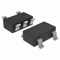
NCP603SN500T1G ON Semiconductor, NCP603SN500T1G Datasheet - Page 4

NCP603SN500T1G
Manufacturer Part Number
NCP603SN500T1G
Description
IC REG LDO 300MA 5.0V SOT23-5
Manufacturer
ON Semiconductor
Datasheet
1.NCP603SN130T1G.pdf
(13 pages)
Specifications of NCP603SN500T1G
Regulator Topology
Positive Fixed
Voltage - Output
5V
Voltage - Input
Up to 6V
Voltage - Dropout (typical)
0.157V @ 300mA
Number Of Regulators
1
Current - Output
300mA (Max)
Current - Limit (min)
300mA
Operating Temperature
-40°C ~ 125°C
Mounting Type
Surface Mount
Package / Case
TSOT-23-5, TSOT-5, TSOP-5
Number Of Outputs
1
Polarity
Positive
Input Voltage Max
6 V
Output Voltage
5 V
Output Type
Fixed
Dropout Voltage (max)
0.125 V at 150 mA
Output Current
300 mA
Line Regulation
10 mV
Load Regulation
45 mV
Voltage Regulation Accuracy
3 %
Maximum Operating Temperature
+ 125 C
Mounting Style
SMD/SMT
Minimum Operating Temperature
- 40 C
Lead Free Status / RoHS Status
Lead free / RoHS Compliant
Available stocks
Company
Part Number
Manufacturer
Quantity
Price
Company:
Part Number:
NCP603SN500T1G
Manufacturer:
VIS
Quantity:
2 622
Part Number:
NCP603SN500T1G
Manufacturer:
ON/安森美
Quantity:
20 000
General
Chip Enable
Timing
ELECTRICAL CHARACTERISTICS
C
10. Performance guaranteed over the indicated operating temperature range by design and/or characterization, production tested at T
11. Values based on design and/or characterization.
Output Noise Voltage (Note 11)
Output Short Circuit Current
Dropout Voltage
Dropout Voltage
Output Current Limit (Note 11)
Disable Current
Ground Current
Thermal Shutdown Temperature (Note 11)
Thermal Shutdown Hysteresis (Note 11)
ADJ Input Bias Current
ENABLE Input Threshold Voltage
Enable Input Bias Current (Note 11)
Output Turn On Time (Note 11)
in
= 25°C. Low duty cycle pulse techniques are used during testing to maintain the junction temperature as close to ambient as possible.
= C
out
=1.0 mF, for typical values T
1.3 V
1.5 V
1.8 V
2.5 V
2.7 V to 5.0 V
1.3 V
1.5 V
1.8 V
2.5 V
2.7 V to 5.0 V
Voltage Increasing, Logic High
Voltage Decreasing, Logic Low
1.25 V to 3.5 V
5.0 V
Characteristic
A
= 25°C, for min/max values T
(V
I out(max)
in
Symbol
V
= 1.750 V, V
I
V
V
I
I
T
T
th(EN)
GND
I
t
V n
I sc
ADJ
DIS
EN
EN
DO
DO
SD
SH
http://onsemi.com
f = 10 Hz to 100 kHz
Measured at: V
I out = 150 mA
Measured at: V out – 2.0%
I out = 300 mA
ENABLE = 0 V, Vin = 6 V
−40°C ≤ T
ENABLE = 0.9 V,
I out = 1.0 mA to 300 mA
ENABLE = 0 V to V in
out
= 1.250 V (adjustable version)), (V
4
A
Test Conditions
= −40°C to 125°C, unless otherwise specified.) (Note 10)
A
≤ 85°C
out
– 2.0%
−0.75
in
Min
350
300
0.9
−
−
−
−
−
−
−
−
−
−
−
−
−
−
−
−
−
−
−
= V
out
+ 0.5 V (fixed version)),
0.01
Typ
650
175
150
125
375
350
245
187
157
650
145
175
3.0
50
85
75
10
15
30
−
−
−
Max
0.75
900
250
225
175
175
125
480
400
340
275
230
180
100
1.0
0.4
25
50
−
−
−
−
−
mV
Unit
J
mA
mV
mV
mA
nA
mA
mA
°C
°C
mA
ms
V
= T
rms
A


