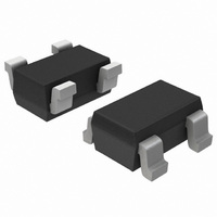
NCP663SQ50T1G ON Semiconductor, NCP663SQ50T1G Datasheet

NCP663SQ50T1G
Specifications of NCP663SQ50T1G
NCP663SQ50T1GOSTR
Available stocks
Related parts for NCP663SQ50T1G
NCP663SQ50T1G Summary of contents
Page 1
... Hand−Held Instruments • Camcorders and Cameras • Automotive Infotainment *For additional information on our Pb−Free strategy and soldering details, please download the ON Semiconductor Soldering and Mounting Techniques Reference Manual, SOLDERRM/D. © Semiconductor Components Industries, LLC, 2009 March, 2009 − Rev. 2 http://onsemi.com 4 SC82− ...
Page 2
GND Enable Input out + C1 This device contains 28 active transistors Figure 1. NCP662/NCV662 Typical Application Diagram Á Á Á Á Á Á Á Á Á Á Á Á Á Á Á Á Á Á Á ...
Page 3
ELECTRICAL CHARACTERISTICS ( 1 out(nom.) enable in in Characteristic Output Voltage (I = 1.0 mA) out NCP662/NCP663 −40°C to 85°C A NCV662/NCV663 −40°C to 125°C A ...
Page 4
3.0 V 2.7 OUT OUT 2.5 2.3 2.1 1.9 1.7 −60 −40 − TEMPERATURE (°C) Figure 3. Quiescent Current versus Temperature 3.020 3.015 3.010 ...
Page 5
V = 3.0 V OUT C = 0.1 mF −0.5 OUT OUT − 100 150 200 250 300 350 t, TIME (ms) Figure 9. Line Transient Response ...
Page 6
Load Regulation The change in output voltage for a change in output current at a constant temperature. Dropout Voltage The input/output differential at which the regulator output no longer maintains regulation against further reductions in input voltage. Measured when the ...
Page 7
A typical application circuit for the NCP662/NCV662 and NCP663/NCV663 series are shown in Figure 1 and Figure 2. Input Decoupling (C1) A 1.0 mF capacitor, either ceramic or tantalum is recommended and should be connected close to the device package. ...
Page 8
... NCP663SQ25T1G NCP663SQ27T1 NCP663SQ27T1G NCP663SQ28T1 NCP663SQ28T1G NCP663SQ30T1 NCP663SQ30T1G NCP663SQ33T1 NCP663SQ33T1G NCP663SQ50T1 NCP663SQ50T1G †For information on tape and reel specifications, including part orientation and tape sizes, please refer to our Tape and Reel Packaging Specifications Brochure, BRD8011/D. ORDERING INFORMATION Marking 1.5 LGY 1.5 LGY 1.8 LGZ 1 ...
Page 9
Nominal Output Voltage Device NCV662SQ15T1 NCV662SQ15T1G NCV662SQ18T1 NCV662SQ18T1G NCV662SQ25T1 NCV662SQ25T1G NCV662SQ27T1 NCV662SQ27T1G NCV662SQ28T1 NCV662SQ28T1G NCV662SQ30T1 NCV662SQ30T1G NCV662SQ33T1 NCV662SQ33T1G NCV662SQ50T1 NCV662SQ50T1G NCV663SQ15T1 NCV663SQ15T1G NCV663SQ18T1 NCV663SQ18T1G NCV663SQ25T1 NCV663SQ25T1G NCV663SQ27T1 NCV663SQ27T1G NCV663SQ28T1 NCV663SQ28T1G NCV663SQ30T1 NCV663SQ30T1G NCV663SQ33T1 NCV663SQ33T1G NCV663SQ50T1 NCV663SQ50T1G †For information on tape ...
Page 10
... *For additional information on our Pb−Free strategy and soldering details, please download the ON Semiconductor Soldering and Mounting Techniques Reference Manual, SOLDERRM/D. ON Semiconductor and are registered trademarks of Semiconductor Components Industries, LLC (SCILLC). SCILLC reserves the right to make changes without further notice to any products herein. SCILLC makes no warranty, representation or guarantee regarding the suitability of its products for any particular purpose, nor does SCILLC assume any liability arising out of the application or use of any product or circuit, and specifically disclaims any and all liability, including without limitation special, consequential or incidental damages. “ ...


