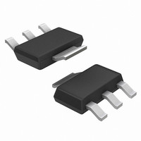
MC33375ST-3.3T3G ON Semiconductor, MC33375ST-3.3T3G Datasheet - Page 3

MC33375ST-3.3T3G
Manufacturer Part Number
MC33375ST-3.3T3G
Description
IC REG LDO 300MA 3.3V SOT223
Manufacturer
ON Semiconductor
Datasheet
1.MC33375ST-1.8T3G.pdf
(14 pages)
Specifications of MC33375ST-3.3T3G
Regulator Topology
Positive Fixed
Voltage - Output
3.3V
Voltage - Input
Up to 13V
Voltage - Dropout (typical)
0.26V @ 300mA
Number Of Regulators
1
Current - Output
300mA (Max)
Operating Temperature
-40°C ~ 125°C
Mounting Type
Surface Mount
Package / Case
SOT-223 (3 leads + Tab), SC-73, TO-261
Number Of Outputs
1
Polarity
Positive
Input Voltage Max
13 V
Output Voltage
3.3 V
Output Type
Fixed
Dropout Voltage (max)
0.1 V at 10 mA
Output Current
300 mA
Line Regulation
10 mV
Load Regulation
25 mV
Voltage Regulation Accuracy
1 %
Maximum Operating Temperature
+ 125 C
Mounting Style
SMD/SMT
Minimum Operating Temperature
- 40 C
Lead Free Status / RoHS Status
Lead free / RoHS Compliant
Current - Limit (min)
-
Lead Free Status / Rohs Status
Lead free / RoHS Compliant
Other names
MC33375ST-3.3T3GOS
MC33375ST-3.3T3GOS
MC33375ST-3.3T3GOSTR
MC33375ST-3.3T3GOS
MC33375ST-3.3T3GOSTR
Available stocks
Company
Part Number
Manufacturer
Quantity
Price
Part Number:
MC33375ST-3.3T3G
Manufacturer:
ON/安森美
Quantity:
20 000
1. Low duty pulse techniques are used during test to maintain junction temperature as close to ambient as possible.
2. Quiescent Current is measured where the PNP pass transistor is in saturation. V
3. For 1.8 V version V
ELECTRICAL CHARACTERISTICS
CURRENT PARAMETERS
ON/OFF INPUTS
THERMAL SHUTDOWN
Output Voltage
Line Regulation
Load Regulation
Dropout Voltage (Note 3)
Ripple Rejection (120 Hz)
Output Noise Voltage
Quiescent Current ON Mode
Quiescent Current OFF Mode
Quiescent Current ON Mode SAT
Current Limit
On/Off Input Voltage
Thermal Shutdown
1.8 V Suffix
2.5 V Suffix
3.0 V Suffix
3.3 V Suffix
5.0 V Suffix
1.8 V Suffix
2.5 V Suffix
3.0 V Suffix
3.3 V Suffix
5.0 V Suffix
I
I
I
I
C
C
1.8 V Suffix
2.5 V Suffix
3.0 V Suffix
3.3 V Suffix
5.0 V Suffix
Logic “1” (Regulator On) V
Logic “0” (Regulator Off) V
Logic “0” (Regulator Off) V
O
O
O
O
L
L
= 10 mA
= 100 mA
= 250 mA
= 300 mA
= 1.0 mF
= 200 mF
I
T
V
2% Tolerance from T
V
All Suffixes T
V
All Suffixes T
T
I
O
O
A
J
DO
in
in
in
= 0 mA to 250 mA
= 50 mA (10 Hz to 100 kHz)
= −40°C to +125°C
= 25°C, V
= [V
= [V
= [V
is constrained by the minimum input voltage of 2.5 V.
O
O
O
V
out
out
out
+ 1] V, 0 < I
+ 1] V to 12 V, I
+ 1] V, I
Characteristic
in(peak−peak)
= V
< 0.03 V
< 0.05 V (1.8 V Option)
in
A
A
= 25°C
= 25°C
= [V
O
V
V
V
O
± 2%
in
in
in
O
= 0 mA to 250 mA,
= [V
= [V
= [V
J
+ 1] V
O
(C
= −40 to +125°C
< 100 mA
= [V
L
O
O
O
O
= 1.0 mF, T
+ 1] V, I
− 0.5] V, I
+ 1] V, V
= 250 mA,
O
+ 1.5] V to [V
O
O
O
A
= 0 mA
Shorted
http://onsemi.com
= 25°C, for min/max values T
= 0 mA (Note 2)
O
+ 5.5] V
3
Symbol
V
Reg
Reg
V
in
I
I
I
I
QSAT
LIMIT
QOn
QOff
CTRL
V
V
in
− V
−
−
O
load
n
line
= [V
O
J
O
= −40°C to +125°C, Note 1)
− 0.5] V guarantees this condition.
1.782
2.475
2.970
3.267
4.950
1.764
2.450
2.940
3.234
4.900
Min
2.4
65
−
−
−
−
−
−
−
−
−
−
−
−
−
−
−
−
−
−
−
1500
1500
1500
1100
1100
1.80
2.50
3.00
3.30
5.00
Typ
115
220
260
160
125
450
150
2.0
5.0
0.3
25
75
46
−
−
−
−
−
−
−
−
1.818
2.525
3.030
3.333
1.836
2.550
3.060
3.366
5.100
1500
1500
2000
2000
2000
Max
5.05
100
200
400
500
200
4.0
0.5
0.3
10
25
−
−
−
−
−
−
mVrms
Unit
Vdc
mV
mV
mV
mA
dB
mA
mA
mA
°C
V


