NCV553SQ50T1G ON Semiconductor, NCV553SQ50T1G Datasheet
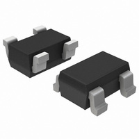
IC REG LDO 80MA NOCAP 5V SC82AB

NCV553SQ50T1G

Manufacturer Part Number
NCV553SQ50T1G
Description
IC REG LDO 80MA NOCAP 5V SC82AB
Manufacturer
ON Semiconductor
Series
NOCAP™r
Datasheet

Specifications of NCV553SQ50T1G

Regulator Topology
Positive Fixed
Voltage - Output
5V
Voltage - Input
Up to 12V
Voltage - Dropout (typical)
0.47V @ 80mA
Number Of Regulators
1
Current - Output
180mA
Operating Temperature
-40°C ~ 125°C
Mounting Type
Surface Mount
Package / Case
SC-70-4, SC-82-4, SOT-323-4, SOT-343
Number Of Outputs
1
Polarity
Positive
Input Voltage Max
12 V
Output Voltage
5 V
Output Type
Fixed
Dropout Voltage (max)
0.8 V at 80 mA
Output Current
180 mA
Line Regulation
4.5 mV / V
Load Regulation
0.8 mV / mA
Voltage Regulation Accuracy
2 %
Maximum Operating Temperature
+ 125 C
Mounting Style
SMD/SMT
Minimum Operating Temperature
- 40 C
Lead Free Status / RoHS Status
Lead free / RoHS Compliant
Current - Limit (min)
-
Lead Free Status / Rohs Status
Lead free / RoHS Compliant
Other names
NCV553SQ50T1G
NCV553SQ50T1GOSTR

Available stocks

Company
Part Number
Manufacturer
Quantity
Price
Part Number:
NCV553SQ50T1G
Manufacturer:
ON/安森美
Quantity:
20 000
Company:
Part Number:
NCV553SQ50T1G
Quantity:
50
NCP552, NCP553, NCV553
80 mA CMOS Low Iq
NOCAPE Voltage Regulator
for handheld communication equipment and portable battery powered
applications which require low quiescent. This series features an
ultra−low quiescent current of 2.8 mA. Each device contains a voltage
reference unit, an error amplifier, a PMOS power transistor, resistors
for setting output voltage, current limit, and temperature limit
protection circuits. The NCP552 series provides an enable pin for
ON/OFF control.
cost ceramic capacitors. The devices have the ability to operate
without an output capacitor. The devices are housed in the
micro−miniature SC82−AB surface mount package. Standard voltage
versions are 1.5, 1.8, 2.5, 2.7, 2.8, 3.0, 3.3, and 5.0 V. Other voltages
are available in 100 mV steps.
Features
Typical Applications
September, 2004 − Rev. 5
This series of fixed output NOCAP linear regulators are designed
These voltage regulators have been designed to be used with low
and Control Changes
Pb−Free Packages are Available*
Low Quiescent Current of 2.8 mA Typical
Low Output Voltage Option
Output Voltage Accuracy of 2.0%
Industrial Temperature Range of −40 C to 85 C
NCP552 Provides an Enable Pin
Battery Powered Consumer Products
Hand−Held Instruments
Camcorders and Cameras
NCV Prefix for Automotive and Other Applications Requiring Site
Semiconductor Components Industries, LLC, 2004
(NCV553, T
Figure 1. NCP552 Typical Application Diagram
Input
Input
Figure 2. NCP553 Typical Application Diagram
C1
C1
This device contains 32 active transistors
+
+
A
= −40 C to +125 C)
GND Enable
V
GND
V
in
in
V
V
N/C
out
out
OFF
ON
+
+
C2
C2
Output
Output
1
See detailed ordering and shipping information in the package
dimensions section on page 8 of this data sheet.
*For additional information on our Pb−Free strategy
and soldering details, please download the
ON Semiconductor Soldering and Mounting
Techniques Reference Manual, SOLDERRM/D.
ORDERING INFORMATION
GND
GND 1
(NCP553, NCV553 Top View)
MARKING DIAGRAMS
PIN CONNECTIONS &
V
V
in
in
http://onsemi.com
http://onsemi.com
SC82−AB (SC70−4)
(NCP552 Top View)
xxx = Device Code
M
1
2
2
4
CASE 419C
SQ SUFFIX
= Date Code
Publication Order Number:
1
4
3
4
3
Enable
V
N/C
V
out
out
NCP552/D

Related parts for NCV553SQ50T1G

NCV553SQ50T1G Summary of contents

Page 1

... ORDERING INFORMATION See detailed ordering and shipping information in the package dimensions section on page 8 of this data sheet. *For additional information on our Pb−Free strategy and soldering details, please download the ON Semiconductor Soldering and Mounting Techniques Reference Manual, SOLDERRM/D. Publication Order Number: NCP552/D ...

Page 2

PIN FUNCTION DESCRIPTION NCP552 NCP553 Pin Name 1 1 GND Power supply ground Vin Positive power supply input voltage Vout Regulated output voltage. 4 − Enable This input is used to place the device into low−power ...

Page 3

ELECTRICAL CHARACTERISTICS otherwise noted.) Characteristic Output Voltage ( mA) out A 1.5 V 1.8 V 2.5 V 2.7 V 2.8 V 3.0 V 3.3 V 5.0 V Output Voltage (T = − ...

Page 4

Load Regulation The change in output voltage for a change in output current at a constant temperature. Dropout Voltage The input/output differential at which the regulator output no longer maintains regulation against further reductions in input voltage. Measured when the ...

Page 5

V = 3.0 V 0.9 out(nom.) 0.8 0 0.6 0.5 0 0.3 0.2 0.1 0 −50 − TEMPERATURE (_C) Figure 3. Dropout Voltage versus Temperature 3. out 3 ...

Page 6

TIME (ms) Figure 9. Load Transient Response out 0 out ...

Page 7

A typical application circuit for the NCP552 series and NCP553 series is shown in Figure 1 and Figure 2, front page. Input Decoupling (C1) A 1.0 mF capacitor either ceramic or tantalum is recommended and should be connected close to ...

Page 8

... NCV553SQ50T1 (Note 6) †For information on tape and reel specifications, including part orientation and tape sizes, please refer to our Tape and Reel Packaging Specifications Brochure, BRD8011/D. 5. Additional voltages in 100 mV steps are available upon request by contacting your ON Semiconductor representative. 6. Automotive qualified. NCP552, NCP553, NCV553 ...

Page 9

NCP552, NCP553, NCV553 PACKAGE DIMENSIONS SC82−AB (SC70−4) SQ SUFFIX CASE 419C−02 ISSUE C NOTES: 1. DIMENSIONING AND TOLERANCING PER ANSI Y14.5M, 1982. 2. CONTROLLING ...

Page 10

... Fax: 480−829−7709 or 800−344−3867 Toll Free USA/Canada Email: orderlit@onsemi.com NCP552, NCP553, NCV553 N. American Technical Support: 800−282−9855 Toll Free USA/Canada Japan: ON Semiconductor, Japan Customer Focus Center 2−9−1 Kamimeguro, Meguro−ku, Tokyo, Japan 153−0051 Phone: 81−3−5773−3850 http://onsemi.com 10 ON Semiconductor Website: http://onsemi ...

Related keywords