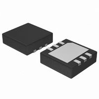
NCP623MN-28R2G ON Semiconductor, NCP623MN-28R2G Datasheet - Page 6

NCP623MN-28R2G
Manufacturer Part Number
NCP623MN-28R2G
Description
IC REG LDO 150MA 2.8V 6-DFN
Manufacturer
ON Semiconductor
Datasheet
1.NCP623MN-25R2G.pdf
(16 pages)
Specifications of NCP623MN-28R2G
Regulator Topology
Positive Fixed
Voltage - Output
2.8V
Voltage - Input
Up to 12V
Voltage - Dropout (typical)
0.18V @ 150mA
Number Of Regulators
1
Current - Output
150mA
Current - Limit (min)
175mA
Operating Temperature
-40°C ~ 85°C
Mounting Type
Surface Mount
Package / Case
6-VFDFN Exposed Pad
Lead Free Status / RoHS Status
Lead free / RoHS Compliant
to reduce the dynamic impedance of the supply rail that
feeds the component. A 1.0 mF capacitor either ceramic or
tantalum is recommended and should be connected close to
the NCP623 package. Higher values will correspondingly
improve the overall line transient response.
ranging from a few mW up to 3.0 W can safely be used. The
minimum decoupling value is 1.0 mF and can be augmented
to fulfill stringent load transient requirements. The regulator
works with ceramic chip capacitors as well as tantalum
devices.
is a true low−noise regulator. With a 10 nF bypass capacitor,
it typically reaches 25 mVRMS overall noise between 100
Hz and 100 kHz. Spectral density graphics as well as noise
dependency versus bypass capacitor information is included
in this datasheet.
NCP623 as depicted by the data−sheet curves. A typical
1.0 ms settling time is achieved with a 10 nF bypass
capacitor. However, due to its low−noise architecture, the
NCP623 can operate without bypass and thus offers a typical
20 ms startup phase. In that case, the typical output noise
stays lower than 65 mVRMS between 100 Hz − 100 kHz.
functions. The output current is internally limited to a
minimum of 175 mA while temperature shutdown occurs if
the die heats up beyond 150°C. These value lets you assess
the maximum differential voltage the device can sustain at
a given output current before its protections come into play.
by:
If T
dissipate up to 595 mW @ 25°C.
from the following formula:
or
Input Decoupling − As with any regulator, it is necessary
Output Decoupling − Output capacitors exhibiting ESRs
Noise Performances − Unlike other LDOs, the NCP623
The bypass capacitor impacts the startup phase of the
Protections − The NCP623 includes several protections
The maximum dissipation the package can handle is given
The power dissipated by the NCP623 can be calculated
Jmax
Ptot + V
Vin max +
is internally limited to 150°C, then the NCP623 can
P max +
in
Ptot ) V out @ I out
@ I
I
T
gnd
gnd
Jmax
R
(I out ) ) V
qJA
) I out
– T
A
in
* V out @ I out
APPLICATION HINTS
http://onsemi.com
6
is extracted from the data−sheet curves: 6.5 mA @ 150 mA.
For a NCP623NW28R2 (2.8 V), the maximum input voltage
will then be 6.48 V, a rather comfortable margin.
typical application for the NCP623 where both input/output
decoupling capacitors appear.
Output
If a 150 mA output current is needed, the ground current
Typical Application − The following figure portraits the
Input
Figure 2. A Typical NCP623 Application with
Figure 3. A Typical NCP623 Application with
Recommended Capacitor Values (Micro8)
Recommended Capacitor Values (DFN6)
C2
1.0 mF
C3
1.0 mF
On/Off
10 nF
C1
8
1
6
1
NC NC
NCP623
7
2
NCP623
5
2
6
3
5
4
4
3
On/Off
C1
10 nF
C3
1.0 mF
C2
1.0 mF
Output
Input


