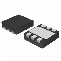
NCP693HMN33TCG ON Semiconductor, NCP693HMN33TCG Datasheet - Page 2

NCP693HMN33TCG
Manufacturer Part Number
NCP693HMN33TCG
Description
IC REG LDO 1A 3.3V CMOS 6-UDFN
Manufacturer
ON Semiconductor
Datasheet
1.NCP693HMN33TCG.pdf
(12 pages)
Specifications of NCP693HMN33TCG
Regulator Topology
Positive Fixed
Voltage - Output
3.3V
Voltage - Input
Up to 6.5V
Voltage - Dropout (typical)
0.43V @ 1A
Number Of Regulators
1
Current - Output
1A
Operating Temperature
-40°C ~ 85°C
Mounting Type
Surface Mount
Package / Case
6-USDFN Exposed Pad
Lead Free Status / RoHS Status
Lead free / RoHS Compliant
Current - Limit (min)
-
Available stocks
Company
Part Number
Manufacturer
Quantity
Price
Company:
Part Number:
NCP693HMN33TCG
Manufacturer:
ON Semiconductor
Quantity:
3 000
Stresses exceeding Maximum Ratings may damage the device. Maximum Ratings are stress ratings only. Functional operation above the
Recommended Operating Conditions is not implied. Extended exposure to stresses above the Recommended Operating Conditions may affect
device reliability.
1. This device series contains ESD protection and exceeds the following tests:
NOTE:
Vin
Vin
CE
PIN FUNCTION DESCRIPTION
MAXIMUM RATINGS
THERMAL CHARACTERISTICS
Input Voltage
Enable Voltage
Output Voltage
Operating Junction Temperature
Operating Ambient Temperature
Storage Temperature
Junction−to−Ambient
PSIJ−Lead 2
Power Dissipation
Pin No.
Human Body Model 2000 V per (JEDEC 22−A114−B)
Machine Model Method 200 V
EP
1
2
3
4
5
6
Single component mounted on an 80 x 80 x 1.5 mm FR4 PCB with stated copper head spreading area. Using the following
boundary conditions as stated in EIA/JESD 51−1, 2, 3, 7, 12.
Version H (NCP693HMNxxTCG)
Vref
Pin Name
Thermal Shutdown
Current Limit &
GND
GND
V
V
CE
Rating
Rating
V
V
out
out
in
in
Regulated output voltage.
Regulated output voltage.
Power supply ground.
This input is used to place the device into low−power standby. When this input is pulled low, the device
is disabled. If this function is not used, Enable should be connected to V
Positive power supply input voltage.
Positive power supply input voltage.
Power supply ground.
Figure 1. Internal Block Diagram
Vout
Vout
GND
http://onsemi.com
Symbol
Symbol
Y
R
V
V
T
V
P
T
T
J−L2
stg
qJA
CE
out
in
A
J
D
2
Vin
Vin
CE
1 oz Copper Thickness, 100 mm
1 oz Copper Thickness, 100 mm
Description
Test Conditions
Vref
Version D (NCP693DMNxxTCG)
Thermal Shutdown
−0.3 to V
Current Limit &
−55 to +125
−40 to +85
−0.3 to V
Value
+150
7
in
+ 0.3
in
2
2
in
.
Typical Value
114
880
25
°C/W
°C/W
Unit
Unit
mW
°C
°C
°C
V
V
V
Vout
Vout
GND


