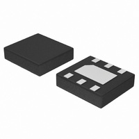
NCP565MNADJT2G ON Semiconductor, NCP565MNADJT2G Datasheet - Page 7

NCP565MNADJT2G
Manufacturer Part Number
NCP565MNADJT2G
Description
IC REG LDO 1.5A ADJ 6-DFN
Manufacturer
ON Semiconductor
Datasheet
1.NCP565V12EVB.pdf
(17 pages)
Specifications of NCP565MNADJT2G
Regulator Topology
Positive Adjustable
Voltage - Output
0.9 ~ 7.7 V
Voltage - Input
2.5 ~ 9 V
Voltage - Dropout (typical)
0.9V @ 1.5A
Number Of Regulators
1
Current - Output
1.5A
Current - Limit (min)
1.6A
Operating Temperature
-40°C ~ 125°C
Mounting Type
Surface Mount
Package / Case
6-VSDFN Exposed Pad
Number Of Outputs
1
Polarity
Positive
Input Voltage Max
9 V
Output Voltage
0.9 V to 7.7 V
Output Type
Adjustable
Dropout Voltage (max)
1.3 V at 1500 mA
Output Current
1.5 A
Line Regulation
0.03 %
Load Regulation
0.03 %
Maximum Operating Temperature
+ 125 C
Mounting Style
SMD/SMT
Minimum Operating Temperature
- 40 C
Reference Voltage
0.927 V
Lead Free Status / RoHS Status
Lead free / RoHS Compliant
Other names
NCP565MNADJT2G
NCP565MNADJT2GOSTR
NCP565MNADJT2GOSTR
Available stocks
Company
Part Number
Manufacturer
Quantity
Price
100
90
80
70
60
50
40
30
20
10
0
Start 1.0 kHz
NOTE: Typical characteristics were measured with the same conditions as electrical characteristics.
Figure 17. Noise Density vs. Frequency
FREQUENCY (kHz)
V
V
I
out
in
out
TYPICAL CHARACTERISTICS
= 3.0 V
= 10 mA
= 0.9 V
Stop 100 kHz
http://onsemi.com
7
100
90
80
70
60
50
40
30
20
10
0
Start 1.0 kHz
Figure 18. Noise Density vs. Frequency
FREQUENCY (kHz)
V
V
I
out
in
out
= 3.0 V
= 1.5 A
= 0.9 V
Stop 100 kHz


