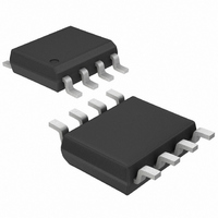
MAX883CSA+T Maxim Integrated Products, MAX883CSA+T Datasheet - Page 7

MAX883CSA+T
Manufacturer Part Number
MAX883CSA+T
Description
IC REG LINEAR 5/ADJ 200MA 8-SOIC
Manufacturer
Maxim Integrated Products
Datasheet
1.MAX882CSA.pdf
(17 pages)
Specifications of MAX883CSA+T
Regulator Topology
Positive Fixed or Adjustable
Voltage - Output
5V, 1.25 ~ 11 V
Voltage - Input
2.7 ~ 11.5 V
Voltage - Dropout (typical)
0.22V @ 200mA
Number Of Regulators
1
Current - Output
200mA
Operating Temperature
0°C ~ 70°C
Mounting Type
Surface Mount
Package / Case
8-SOIC (3.9mm Width)
Number Of Outputs
1
Polarity
Positive
Input Voltage Max
11.5 V
Output Voltage
1.25 V to 11 V, 5 V
Output Type
Adjustable, Fixed
Dropout Voltage (max)
0.22 V at 100 mA
Output Current
200 mA
Line Regulation
40 mV
Load Regulation
100 mV
Voltage Regulation Accuracy
5 %
Maximum Power Dissipation
1.5 W
Maximum Operating Temperature
+ 70 C
Mounting Style
SMD/SMT
Minimum Operating Temperature
0 C
Reference Voltage
1.24 V
Lead Free Status / RoHS Status
Lead free / RoHS Compliant
Current - Limit (min)
-
Lead Free Status / Rohs Status
Lead free / RoHS Compliant
The MAX882/MAX883/MAX884 are micropower, low-
dropout linear regulators designed primarily for battery-
powered applications. They feature Dual Mode operation,
allowing a fixed output of 5V for the MAX883 and 3.3V for
the MAX882/MAX884, or an adjustable output from 1.25V
to 11V. These devices supply up to 200mA while requiring
less than 15µA quiescent current. As illustrated in Figure
1, they consist of a 1.20V reference, error amplifier, MOS-
FET driver, p-channel pass transistor, dual-mode com-
parator, and feedback voltage-divider.
The 1.20V reference is connected to the error amplifier’s
inverting input. The error amplifier compares this refer-
ence with the selected feedback voltage and amplifies
the difference. The MOSFET driver reads the error signal
and applies the appropriate drive to the p-channel pass
transistor. If the feedback voltage is lower than the refer-
ence, the pass transistor’s gate is pulled lower, allowing
more current to pass and increasing the output voltage. If
the feedback voltage is too high, the pass transistor gate
is pulled up, allowing less current to pass to the output.
The output voltage is fed back through either an inter-
nal resistor voltage-divider connected to the OUT pin,
or an external resistor network connected to the SET
pin. The dual-mode comparator examines the SET pin
voltage and selects the feedback path used. If the SET
pin is below 65mV, internal feedback is used and the
output voltage is regulated to 5V for the MAX883 or
_______________Detailed Description
MAX882
3, 6
—
1
2
4
5
7
8
PIN
MAX883/
MAX884
3, 6
—
1
2
4
5
7
8
_______________________________________________________________________________________
NAME
STBY
GND
LBO
OUT
OFF
SET
LBI
IN
5V/3.3V or Adjustable, Low-Dropout,
Low-Battery Output is an open-drain output that goes low when LBI is less than 1.2V. Connect
to IN or OUT through a pull-up resistor. LBO is undefined during shutdown mode
(MAX883/MAX884).
Feedback for setting the output voltage. Connect to GND to set the output voltage to the
preselected 3.3V or 5V. Connect to an external resistor network for adjustable-output operation.
Ground pins—also function as heatsinks in the SO package. All GND pins must be soldered to
the PC board for proper power dissipation. Connect to large copper pads or planes to channel
heat from the IC.
Regulator Output. Fixed or adjustable from 1.25V to 11.0V. Sources up to 200mA. Bypass with a
2.2µF capacitor.
Regulator Input. Supply voltage can range from 2.7V to 11.5V.
Standby. Active-low comparator input. Connect to GND to disable the output or to IN for normal
operation. A resistor network (from IN) can be used to set a standby mode threshold.
Shutdown. Active-low logic input. In OFF mode, supply current is reduced below 1µA and
V
Low-Battery comparator Input. Tie to IN when not used.
OUT
Low I
= 0.
Q
, 200mA Linear Regulators
3.3V for the MAX882/MAX884. Additional blocks
include a foldback current limiter, reverse-current pro-
tection, a thermal sensor, shutdown or standby logic,
and a low-battery-detection comparator.
The MAX882/MAX883/MAX884 feature a 200mA P-
channel MOSFET pass transistor. This provides several
advantages over similar designs using PNP pass tran-
sistors, including longer battery life.
The p-channel MOSFET requires no base drive, which
reduces quiescent current considerably. PNP-based reg-
ulators waste large amounts of current in dropout when
the pass transistor saturates. They also use high base-
drive currents under large loads. The MAX882/MAX883/
MAX884 do not suffer from these problems and consume
only 11µA of quiescent current during light loads, heavy
loads, and dropout.
The MAX882/MAX883/MAX884 feature Dual Mode
operation. In preset voltage mode, the MAX883’s out-
put is set to 5V and the MAX882/MAX884’s output is set
to 3.3V, using internal trimmed feedback resistors.
Select this mode by connecting SET to ground.
In preset voltage mode, impedances between SET and
ground should be less than 100kΩ. Otherwise, spurious
conditions could cause the voltage at SET to exceed
the 65mV dual-mode threshold.
DESCRIPTION
Internal p-Channel Pass Transistor
Output Voltage Selection
Pin Description
7


