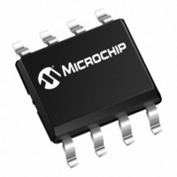
TC1300R-2.8VUA Microchip Technology, TC1300R-2.8VUA Datasheet - Page 2

TC1300R-2.8VUA
Manufacturer Part Number
TC1300R-2.8VUA
Description
IC REG LDO 2.8V 300MA SD 8MSOP
Manufacturer
Microchip Technology
Datasheet
1.TC1300R-2.5VUA.pdf
(16 pages)
Specifications of TC1300R-2.8VUA
Regulator Topology
Positive Fixed
Voltage - Output
2.8V
Voltage - Input
Up to 6V
Voltage - Dropout (typical)
0.21V @ 300mA
Number Of Regulators
1
Current - Output
300mA (Min)
Operating Temperature
-40°C ~ 125°C
Mounting Type
Surface Mount
Package / Case
8-MSOP, Micro8™, 8-uMAX, 8-uSOP,
Number Of Outputs
1
Polarity
Positive
Input Voltage Max
6 V
Output Voltage
2.8 V
Output Type
Fixed
Dropout Voltage (max)
0.03 V at 100 uA
Output Current
300 mA
Line Regulation
0.02 %
Load Regulation
0.5 %
Voltage Regulation Accuracy
0.5 %
Maximum Operating Temperature
+ 125 C
Mounting Style
SMD/SMT
Minimum Operating Temperature
- 40 C
Lead Free Status / RoHS Status
Lead free / RoHS Compliant
Current - Limit (min)
-
Lead Free Status / Rohs Status
Lead free / RoHS Compliant
Other names
TC1300R2.8VUA
Available stocks
Company
Part Number
Manufacturer
Quantity
Price
Part Number:
TC1300R-2.8VUA
Manufacturer:
MICROCHIP/微芯
Quantity:
20 000
Part Number:
TC1300R-2.8VUATR
Manufacturer:
MICR
Quantity:
20 000
TC1300
1.0
Absolute Maximum Ratings*
Input Voltage ....................................................................6.5V
Output Voltage ................................. (V
Power Dissipation ......................... Internally Limited (Note 6)
Operating Junction Temperature, T
Maximum Junction Temperature, Tj .............................. 150°C
Storage Temperature .................................. – 65°C to +150°C
Maximum Voltage on Any Pin ............. (V
*Notice: Stresses above those listed under “maximum rat-
ings” may cause permanent damage to the device. This is a
stress rating only and functional operation of the device at
those or any other conditions above those indicated in the
operational listings of this specification is not implied. Expo-
sure to maximum rating conditions for extended periods may
affect device reliability.
ELECTRICAL CHARACTERISTICS
DS21385C-page 2
V
for junction temperature (Note 8) of -40°C to +125°C.
Input Operating Voltage
Maximum Output Current
Output Voltage
V
Line Regulation
Load Regulation
Note 1: V
IN
OUT
= V
Temperature Coefficient
2:
3: Regulation is measured at a constant junction temperature using low duty cycle pulse testing. Load regulation is tested
4: Dropout voltage is defined as the input to output differential at which the output voltage drops 2% below its nominal value
5: Thermal Regulation is defined as the change in output voltage at a time t after a change in power dissipation is applied,
6: The maximum allowable power dissipation is a function of ambient temperature, the maximum allowable junction tem-
7: The minimum V
8: The junction temperature of the device is approximated by soaking the device under test at an ambient temperature
OUT
ELECTRICAL
CHARACTERISTICS
Parameters
over a load range from 0.1 mA to the maximum specified output current. Changes in output voltage due to heating
effects are covered by the thermal regulation specification.
measured at a 1V differential.
excluding load or line regulation effects. Specifications are for a current pulse equal to I
perature and the thermal resistance from junction-to-air (i.e. T
pation causes the device to initiate thermal shutdown. Please see Section 4.0, “Thermal Considerations”, of this data
sheet for more details.
equal to the desired junction temperature. The test time is small enough such that the rise in the junction temperature
over the ambient temperature is not significant.
+ 1V, I
TCV
R
is the regulator output voltage setting.
OUT
L
= 0.1 mA, C
=
------------------------------------------------------------------------------------- -
V O UTMAX V OUTMIN
IN
has to meet two conditions: V
L
V
= 3.3 µF, SHDN > V
OUT
J
–
....... – 40°C < T
V
V
I
SS
OUT MAX
V
OUT
OUT
V
Sym
OUT
V
SS
OUT
- 0.3) to (V
T
IN
/V
/ V
-0.3) to (V
/ T
OUT
IN
10
6
J
V
IN
< 150°C
R
IN
IH
+ 0.3)
Min
300
2.7
- 2.5%
+0.3)
, T
—
—
—
—
A
IN
= 25°C, unless otherwise noted. BOLDFACE type specifications apply
2.7V and V
V
R
0.02
Typ
0.5
± 0.5%
25
—
—
—
PIN DESCRIPTIONS
A
RESET
Bypass
SHDN
, T
V
V
GND
IN
Pin
V
NC
OUT
DET
J
IN
,
V
(V
R
JA
Max
0.35
R
+ 2.5%
6.0
2.0
). Exceeding the maximum allowable power dissi-
—
—
—
+ V
RESET output remains low while V
below the reset voltage threshold and for
300 msec after V
old.
Regulated Voltage Output
Ground Terminal
Reference Bypass Input. Connecting an
optional 470 pF to this input further reduces
output noise.
Shutdown Control Input. The regulator is fully
enabled when a logic high is applied to this
input. The regulator enters shutdown when a
logic low is applied to this input. During shut-
down, regulator output voltage falls to zero,
RESET output remains valid and supply cur-
rent is reduced to 30 µA (typ.).
No connect
Power Supply Input
Detected Input Voltage. V
connected together.
DROPOUT
ppm/°C Note 2
Units
mA
%
%
V
V
).
L MAX
2002 Microchip Technology Inc.
Note 7
Note 1
(V
I
DET
Description
L
R
= 0.1 mA to I
at V
+ 1V) < V
rises above reset thesh-
IN
DET
Conditions
= 6V for t = 10 msec.
and V
IN
OUT
< 6V
DET
MAX,
IN
can be
is
Note 3


