ADG465BRTZ-REEL7 Analog Devices Inc, ADG465BRTZ-REEL7 Datasheet
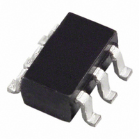
IC CHANNEL PROTECTOR SGL SOT23-6

ADG465BRTZ-REEL7

Manufacturer Part Number
ADG465BRTZ-REEL7
Description
IC CHANNEL PROTECTOR SGL SOT23-6
Manufacturer
Analog Devices Inc
Series
ADG465r
Datasheet

Specifications of ADG465BRTZ-REEL7

Voltage - Clamping
±40V
Technology
Mixed Technology
Number Of Circuits
1
Applications
General Purpose
Package / Case
SOT-23-6
No. Of Channels
1
On State Resistance Max
80ohm
Supply Voltage Range
± 20V
Operating Temperature Range
-40°C To +85°C
Analog Switch Case Style
SOT-23
No. Of Pins
6
Msl
MSL 1 - Unlimited
Operating Temperature (min)
-40C
Operating Temperature (max)
85C
Operating Temperature Classification
Industrial
Mounting
Surface Mount
Pin Count
6
Package
6SOT-23
Lead Free Status / RoHS Status
Lead free / RoHS Compliant
Power (watts)
-
Voltage - Working
-
Lead Free Status / Rohs Status
Compliant
Other names
ADG465BRTZ-REEL7
a
REV. A
Information furnished by Analog Devices is believed to be accurate and
reliable. However, no responsibility is assumed by Analog Devices for its
use, nor for any infringements of patents or other rights of third parties
which may result from its use. No license is granted by implication or
otherwise under any patent or patent rights of Analog Devices.
GENERAL DESCRIPTION
The ADG465 is a single channel protector in an SOT-23 pack-
age. The channel protector is placed in series with the signal
path, and will protect sensitive components from voltage tran-
sience in the signal path whether or not the power supplies are
present. Because the channel protection works regardless of the
presence of the supplies, the channel protectors are ideal for use
in applications where correct power sequencing cannot always
be guaranteed to protect analog inputs (e.g., hot-insertion rack
systems). This is discussed further, and some example circuits
are given, in the Applications section of this data sheet.
A channel protector consists of an n-channel MOSFET, a
p-channel MOSFET and an n-channel MOSFET, connected in
series. The channel protector behaves like a series resistor dur-
ing normal operation, i.e., (V
When a channel’s analog input exceeds the power supplies
(including V
switch off, clamping the output to either V
Circuitry and signal source protection is provided in the event of
an overvoltage or power loss. The channel protectors can with-
stand overvoltage inputs from –40 V to +40 V. See the Circuit
Information section of this data sheet.
The ADG465 can operate from both bipolar and unipolar
supplies. The channels are normally on when power is con-
nected, and open circuit when power is disconnected. With
power supplies of 15 V, the on-resistance of the ADG465 is
80
is disconnected, the input leakage current is approximately
The ADG465 is available in a 6-lead plastic surface mount
SOT-23 package, and an 8-lead SOIC package.
5 nA typ.
FEATURES
Fault and Overvoltage Protection up to
44 V Supply Maximum Ratings
Low On Resistance 80
1 nA Max Path Current Leakage @ +25 C
Low Power Dissipation 0.8 W Typ
Latchup-Proof Construction
APPLICATIONS
ATE Equipment
Sensitive Measurement Equipment
Hot-Insertion Rack Systems
ADC Input Channel Protection
typ, with a leakage current of 1 nA max. When power
Signal Paths Open Circuit with Power Off
Signal Path Resistance of R
DD
and V
SS
= 0 V), one of the MOSFETs will
SS
+ 2 V) < V
Typ
ON
with Power On
IN
SS
< (V
+ 2 V or V
DD
40 V
– 1.5 V).
DD
– 1.5 V.
PRODUCT HIGHLIGHTS
1. Fault Protection.
2. Low Power Dissipation.
3. Low R
4. Trench Isolation Latchup-Proof Construction.
One Technology Way, P.O. Box 9106, Norwood, MA 02062-9106, U.S.A.
Tel: 781/329-4700
Fax: 781/326-8703
V
The ADG465 can withstand continuous voltage inputs from
–40 V to +40 V. When a fault occurs due to the power sup-
plies being turned off, or due to an overvoltage being applied
to the ADG465, the output is clamped. When power is turned
off, current is limited to the nanoampere level.
A dielectric trench separates the p- and n-channel MOSFETs
thereby preventing latchup.
DD
V
IN
ON
V
80
Single Channel Protector
FUNCTIONAL BLOCK DIAGRAM
IN
typ.
in an SOT-23 Package
World Wide Web Site: http://www.analog.com
V
D1
V
ADG465
OUTPUT CLAMPED
@ V
DD
DD
V
SS
– 1.5V
© Analog Devices, Inc., 1998
V
V
S1
DD
ADG465
V
OUT
V
OUT

Related parts for ADG465BRTZ-REEL7

ADG465BRTZ-REEL7 Summary of contents

Page 1

FEATURES Fault and Overvoltage Protection up to Signal Paths Open Circuit with Power Off Signal Path Resistance Supply Maximum Ratings Low On Resistance 80 Typ 1 nA Max Path Current Leakage @ +25 C ...

Page 2

ADG465–SPECIFICATIONS 1 Dual Supply ( –15 V, GND = 0 V, unless otherwise noted Parameter FAULT PROTECTED CHANNEL 2 Fault-Free Analog Signal Range LEAKAGE CURRENTS Channel Output Leakage, I ...

Page 3

ABSOLUTE MAXIMUM RATINGS (T = +25 C unless otherwise noted ...

Page 4

ADG465 —Typical Performance Characteristics 140 TEMP = +25 C 130 120 110 –5V 100 +10V –10V –10 – ...

Page 5

CIRCUIT INFORMATION Figure 6 below shows a simplified schematic of a channel pro- tector circuit. The circuit is comprised of four MOS transis- tors—two NMOS and two PMOS. One of the PMOS devices does not lie directly in the signal ...

Page 6

ADG465 When a negative overvoltage is applied to the channel protector circuit, the PMOS transistor enters a saturated mode of operation as the drain voltage exceeds V – See Figure 9 below the case ...

Page 7

... In addition, TVSs offer no protection against latchup of sensitive CMOS devices when the power supplies are off. To provide the best leakage current specification and circuit protection, the best solution is to use a channel protector in conjunction with a TVS. Figure 13 shows an input protection scheme that uses both a TVS and channel protector ...

Page 8

ADG465 0.071 (1.80) 0.059 (1.50) 0.051 (1.30) 0.035 (0.90) 0.006 (0.15) 0.002 (0.05) OUTLINE DIMENSIONS Dimensions shown in inches and (mm). 6-Lead Plastic Surface Mount SOT-23 Package (RT-6) 0.122 (3.10) 0.106 (2.70 0.118 (3.00) 0.098 (2.50) 1 ...

Related keywords