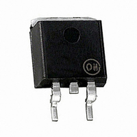
LM317BD2TR4 ON Semiconductor, LM317BD2TR4 Datasheet
LM317BD2TR4
Specifications of LM317BD2TR4
Available stocks


Related parts for LM317BD2TR4


LM317BD2TR4 Summary of contents
Page 1
LM317, NCV317 1.5 A Adjustable Output, Positive Voltage Regulator The LM317 is an adjustable 3−terminal positive voltage regulator capable of supplying in excess of 1.5 A over an output voltage range of 1 This voltage regulator ...
Page 2
MAXIMUM RATINGS Input−Output Voltage Differential Power Dissipation Case 221A T = +25°C A Thermal Resistance, Junction−to−Ambient Thermal Resistance, Junction−to−Case 2 Case 936 (D PAK− +25°C A Thermal Resistance, Junction−to−Ambient Thermal Resistance, Junction−to−Case Operating Junction Temperature Range Storage Temperature ...
Page 3
V 190 3.6 k 5.8 k 110 5.1 k Figure 2. Representative Schematic Diagram Pulse testing required Duty ...
Page 4
LM317 Adjust 0 Adj Load Regulation (mV (min Load (max Load Figure 4. Load Regulation and 0.1 mF ...
Page 5
out -0.8 -1.0 -50 - JUNCTION TEMPERATURE (°C) J Figure 7. Load Regulation 70 ...
Page 6
C 80 Without out I = 500 120 25° 5 OUTPUT VOLTAGE ...
Page 7
Basic Circuit Operation The LM317 is a 3−terminal floating regulator. In operation, the LM317 develops and maintains a nominal 1.25 V reference (V ) between its output and adjustment ref terminals. This reference voltage is converted to a programming current ...
Page 8
Figure 21. D Power Dissipation versus P.C.B. Copper Length LM317 in1 0.1 mF Adjust 1 Current Limit Adjust * Diodes D and D and ...
Page 9
V R +25 V out 1 LM317 1. Adjust R 2 100 * To provide current limiting the system O * ground, the source of the FET must be tied negative voltage ...
Page 10
... ORDERING INFORMATION Device LM317BD2T LM317BD2TG LM317BD2TR4 LM317BD2TR4G LM317BT LM317BTG LM317D2T LM317D2TG LM317D2TR4 LM317D2TR4G LM317T LM317TG NCV317BD2T* NCV317BD2TG* NCV317BD2TR4* NCV317BD2TR4G* NCV317BT* NCV317BTG* †For information on tape and reel specifications, including part orientation and tape sizes, please refer to our Tape and Reel Packaging Specifications Brochure, BRD8011/D. ...
Page 11
... A CHAMFER 0.010 (0.254 16.155 *For additional information on our Pb−Free strategy and soldering details, please download the ON Semiconductor Soldering and Mounting Techniques Reference Manual, SOLDERRM/D. PACKAGE DIMENSIONS 2 D PAK−3 D2T SUFFIX CASE 936−03 ISSUE C −T− TERMINAL SOLDERING FOOTPRINT* 10.49 8 ...
Page 12
... Opportunity/Affirmative Action Employer. This literature is subject to all applicable copyright laws and is not for resale in any manner. PUBLICATION ORDERING INFORMATION LITERATURE FULFILLMENT: Literature Distribution Center for ON Semiconductor P.O. Box 5163, Denver, Colorado 80217 USA Phone: 303−675−2175 or 800−344−3860 Toll Free USA/Canada Fax: 303− ...