CS8371ETVA7G ON Semiconductor, CS8371ETVA7G Datasheet - Page 9
CS8371ETVA7G
Manufacturer Part Number
CS8371ETVA7G
Description
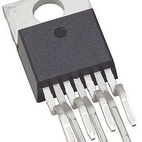
IC REG LIN DUAL 8/5V VRT TO220-7
Manufacturer
ON Semiconductor
Datasheet
1.CS8371ET7.pdf
(11 pages)
Specifications of CS8371ETVA7G
Regulator Topology
Positive Fixed
Voltage - Output
8V, 5V
Voltage - Input
7 ~ 26 V
Number Of Regulators
2
Current - Output
1A, 250mA
Current - Limit (min)
1.1A, 270mA
Operating Temperature
-40°C ~ 85°C
Mounting Type
Through Hole
Package / Case
TO-220-7 (Bent and Staggered Leads)
Polarity
Positive
Number Of Outputs
2
Output Type
Fixed
Output Voltage
5 V, 8 V
Output Current
1 A, 0.25 A
Line Regulation
50 mV
Load Regulation
150 mV
Dropout Voltage (max)
1.2 V
Input Voltage Max
12.5 V
Maximum Operating Temperature
+ 85 C
Minimum Operating Temperature
- 40 C
Mounting Style
Through Hole
Voltage Regulation Accuracy
5 %
Lead Free Status / RoHS Status
Lead free / RoHS Compliant
Voltage - Dropout (typical)
-
Lead Free Status / Rohs Status
Lead free / RoHS Compliant
Other names
CS8371ETVA7GOS


cause small signal oscillations at the output. This will
depend on the load conditions. With these types of loads, a
traditional output stage may be better suited for proper
operation.
Performance Characteristics section for appropriate output
capacitor selections for stability if an external capacitor is
required by the switching characteristics of the load. Output
2 has a Darlington NPN−type output structure and is
inherently stable with any type of capacitive load or no
capacitor at all.
Calculating Power Dissipation in a
Dual Output Linear Regulator
regulator (Figure 24) is
where:
permissible value of R
package section of the data sheet. Those packages with
R
the die temperature below 150°C.
P D(max) + V IN(max) * V OUT1(min) I OUT1(max) )
PACKAGE THERMAL DATA
qJA
Output 1 employs NOCAP. Refer to the plots in the Typical
The maximum power dissipation for a dual output
V
V
V
I
application,
I
application, and
I
I
Once the value of P
The value of R
OUT1(max)
OUT2(max)
Q
OUT(max)
IN(max)
OUT1(min)
OUT2(min)
’s less than the calculated value in equation 2 will keep
is the quiescent current the regulator consumes at
V IN(max) * V OUT2(min) I OUT2(max) ) V IN(max) IQ
is the maximum input voltage,
.
R
R
is the minimum output voltage from V
is the minimum output voltage from V
is the maximum output current, for the
is the maximum output current, for the
qJC
qJA
R qJA +
qJA
can be compared with those in the
qJA
Parameter
D(max)
can be calculated:
150°C * T A
P D
is known, the maximum
Typical
Typical
http://onsemi.com
OUT1
OUT2
(1)
(2)
CS8371
,
,
9
dissipate the heat generated by the IC, and an external
heatsink will be required.
Heat Sinks
package to improve the flow of heat away from the IC and
into the surrounding air.
outside environment will have a thermal resistance. Like
series electrical resistances, these resistances are summed to
determine the value of R
where:
R
functions of the package type, heatsink and the interface
between them. These values appear in heat sink data sheets
of heat sink manufacturers.
qJA
In some cases, none of the packages will be sufficient to
A heat sink effectively increases the surface area of the
Each material in the heat flow path between the IC and the
R
R
R
R
V
IN
qJC
qCS
qSA
qJC
, it too is a function of package type. R
SEVEN LEAD
Figure 24. Dual Output Regulator With Key
appears in the package section of the data sheet. Like
= the junction−to−case thermal resistance,
= the case−to−heatsink thermal resistance, and
= the heatsink−to−ambient thermal resistance.
TO−220
I
IN
Performance Parameters Labeled.
2.4
R qJA + R qJC ) R qCS ) R qSA
50
REGULATOR
Control
Features
SMART
qJA:
I
Q
®
I
I
OUT1
OUT2
qCS
°C/W
°C/W
Unit
and R
V
V
OUT2
qSA
OUT1
are
(3)
Related parts for CS8371ETVA7G
Image
Part Number
Description
Manufacturer
Datasheet
Request
R

Part Number:
Description:
ON Semiconductor [VOLTAGE REGULATOR]
Manufacturer:
ON Semiconductor
Datasheet:
Part Number:
Description:
357-036-542-201 CARDEDGE 36POS DL .156 BLK LOPRO
Manufacturer:
ON Semiconductor
Datasheet:
Part Number:
Description:
357-036-542-201 CARDEDGE 36POS DL .156 BLK LOPRO
Manufacturer:
ON Semiconductor
Datasheet:
Part Number:
Description:
357-036-542-201 CARDEDGE 36POS DL .156 BLK LOPRO
Manufacturer:
ON Semiconductor
Datasheet:
Part Number:
Description:
357-036-542-201 CARDEDGE 36POS DL .156 BLK LOPRO
Manufacturer:
ON Semiconductor
Datasheet:
Part Number:
Description:
357-036-542-201 CARDEDGE 36POS DL .156 BLK LOPRO
Manufacturer:
ON Semiconductor
Datasheet:
Part Number:
Description:
357-036-542-201 CARDEDGE 36POS DL .156 BLK LOPRO
Manufacturer:
ON Semiconductor
Datasheet:
Part Number:
Description:
357-036-542-201 CARDEDGE 36POS DL .156 BLK LOPRO
Manufacturer:
ON Semiconductor
Datasheet:
Part Number:
Description:
357-036-542-201 CARDEDGE 36POS DL .156 BLK LOPRO
Manufacturer:
ON Semiconductor
Datasheet:
Part Number:
Description:
357-036-542-201 CARDEDGE 36POS DL .156 BLK LOPRO
Manufacturer:
ON Semiconductor
Datasheet:
Part Number:
Description:
357-036-542-201 CARDEDGE 36POS DL .156 BLK LOPRO
Manufacturer:
ON Semiconductor
Datasheet:
Part Number:
Description:
Manufacturer:
ON Semiconductor
Datasheet:
Part Number:
Description:
Manufacturer:
ON Semiconductor
Datasheet:
Part Number:
Description:
Manufacturer:
ON Semiconductor
Datasheet: