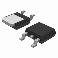
LM317MBDTRK ON Semiconductor, LM317MBDTRK Datasheet - Page 3

LM317MBDTRK
Manufacturer Part Number
LM317MBDTRK
Description
IC REG POS 500MA ADJ 4% DPAK
Manufacturer
ON Semiconductor
Datasheet
1.LM317MDTRKG.pdf
(14 pages)
Specifications of LM317MBDTRK
Regulator Topology
Positive Adjustable
Voltage - Output
1.2 ~ 37 V
Voltage - Input
Up to 40V
Number Of Regulators
1
Current - Output
500mA (Min)
Current - Limit (min)
500mA
Operating Temperature
-40°C ~ 125°C
Mounting Type
Surface Mount
Package / Case
TO-252-2, DPak (2 Leads + Tab), TO-252AA, SC-63
Polarity
Positive
Number Of Outputs
1
Output Type
Adjustable
Output Voltage
1.2 V to 37 V
Output Current
0.25 A
Line Regulation
0.07 % / V
Load Regulation
1.5 % / V
Input Voltage Max
40 V
Maximum Operating Temperature
+ 125 C
Minimum Operating Temperature
- 40 C
Mounting Style
SMD/SMT
Reference Voltage
1.3 V
Voltage Regulation Accuracy
4 %
Lead Free Status / RoHS Status
Contains lead / RoHS non-compliant
Voltage - Dropout (typical)
-
Lead Free Status / Rohs Status
Lead free / RoHS Compliant
Available stocks
Company
Part Number
Manufacturer
Quantity
Price
Company:
Part Number:
LM317MBDTRKG
Manufacturer:
ON Semiconductor
Quantity:
26 295
Part Number:
LM317MBDTRKG
Manufacturer:
ON/安森美
Quantity:
20 000
7. T
8. Load and line regulation are specified at constant junction temperature. Changes in V
9. C
10. Thermal characteristics are not subject to production test.
11. Since Long−Term Stability cannot be measured on each device before shipment, this specification is an engineering estimate of average
ELECTRICAL CHARACTERISTICS
Line Regulation (Note 8) (T
Load Regulation (Note 8)
Adjustment Pin Current
Adjustment Pin Current Change
Reference Voltage
Line Regulation (Note 8)
Load Regulation (Note 8)
Temperature Stability (T
Minimum Load Current to Maintain Regulation (V
Maximum Output Current
RMS Noise, % of V
Ripple Rejection, V
Thermal Shutdown (Note 10)
Long−Term Stability, T
separately. Pulse testing with low duty cycle is used.
stability from lot−to−lot.
T
2.5 V ≤ V
3.0 V ≤ V
3.0 V ≤ V
10 mA ≤ I
V
V
Without C
C
T
low
Adj
A
A
I
I
Adj
V
V
V
V
= 25°C for End−point Measurements
− V
− V
= 25°C, 10 mA ≤ I
, when used, is connected between the adjustment pin and ground.
O
O
O
O
to T
= 10 mF
≤ 5.0 V
≥ 5.0 V
≤ 5.0 V
≥ 5.0 V
O
O
high
≤ 15 V, P
= 40 V, P
I
I
I
−V
O
Adj
− V
− V
≤ 0.5 A
= 0° to +125°C for LM317MA
O
O
O
≤ 40 V
≤ 40 V, 10 mA ≤ I
≤ 40 V, 10 mA ≤ I
O
O
D
D
(T
= 10 V, f = 120 Hz (Note 9)
≤ P
≤ P
J
O
A
Characteristics
= T
low
max
max
= 25°C, 10 Hz ≤ f ≤ 10 kHz)
≤ 0.5 A
A
high
≤ T
, T
= 25°C, 3.0 V ≤ V
J
A
(Note 11)
≤ T
= 25°C
high
L
L
≤ 0.5 A, P
≤ 0.5 A, P
)
(V
I
− V
I
D
D
T
O
− V
≤ P
I
≤ P
low
= 5.0 V; I
− V
O
max
max
to T
≤ 40 V)
O
= 40 V)
high
http://onsemi.com
O
= − 40° to +125°C for LM317MAB, NCV317MAB.
= 0.1 A, T
3
Figure
3, 4
3
4
5
5
3
4
5
5
5
−
6
−
5
J
= T
low
Symbol
Reg
Reg
Reg
Reg
DI
I
to T
I
V
I
Lmin
RR
max
T
Adj
N
S
−
ref
Adj
S
load
load
line
line
high
O
(Note 7), unless otherwise noted.)
LM317MA / LM317MAB/NCV317MAB
due to heating effects must be taken into account
1.225
0.15
Min
0.5
66
−
−
−
−
−
−
−
−
−
−
−
−
−
−
1.250
0.01
0.02
0.25
Typ
180
5.0
0.1
0.2
0.3
0.7
3.5
0.9
0.3
50
20
65
80
−
1.275
Max
0.04
0.07
100
0.5
5.0
1.5
1.0
25
70
10
−
−
−
−
−
−
−
% V
% V
% V
% V
%/1.0
kHrs.
Unit
%/V
%/V
mV
mV
mA
mA
mA
dB
°C
V
A
O
O
O
O


