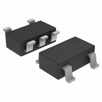
NCP360SNAET1G ON Semiconductor, NCP360SNAET1G Datasheet - Page 2

NCP360SNAET1G
Manufacturer Part Number
NCP360SNAET1G
Description
IC CTLR USB POS OVP FET SOT23-5
Manufacturer
ON Semiconductor
Type
Power Supply Controllerr
Datasheet
1.NCP360SNAET1G.pdf
(13 pages)
Specifications of NCP360SNAET1G
Voltage - Working
1.2 ~ 20V
Voltage - Clamping
7.4V
Technology
Mixed Technology
Number Of Circuits
1
Applications
USB
Package / Case
TSOT-23-5, TSOT-5, TSOP-5
Number Of Voltages Monitored
1
Monitored Voltage
1.2 V to 20 V
Manual Reset
No
Watchdog
No
Supply Voltage (max)
20 V
Supply Voltage (min)
1.2 V
Mounting Style
SMD/SMT
Maximum Operating Temperature
+ 85 C
Minimum Operating Temperature
- 40 C
Lead Free Status / RoHS Status
Lead free / RoHS Compliant
Power (watts)
-
Lead Free Status / Rohs Status
Lead free / RoHS Compliant
Other names
NCP360SNAET1G
NCP360SNAET1GOSTR
NCP360SNAET1GOSTR
Available stocks
Company
Part Number
Manufacturer
Quantity
Price
Company:
Part Number:
NCP360SNAET1G
Manufacturer:
AAT
Quantity:
4 600
Company:
Part Number:
NCP360SNAET1G
Manufacturer:
ON
Quantity:
3 000
Part Number:
NCP360SNAET1G
Manufacturer:
ON/安森美
Quantity:
20 000
PIN FUNCTION DESCRIPTION (UDFN6 Package)
PIN FUNCTION DESCRIPTION (TSOP−5 Package)
Pin No.
Pin No.
4, 5
1
2
3
6
−
1
2
3
4
5
Name
FLAG
Name
FLAG
PAD1
GND
OUT
GND
OUT
EN
EN
IN
IN
GND
EN
OUTPUT
OUTPUT
OUTPUT
OUTPUT
IN
POWER
POWER
POWER
POWER
POWER
INPUT
INPUT
Type
Type
1
2
3
UDFN6
PAD1
Enable Pin. The device enters in shutdown mode when this pin is tied to a high level. In this case the
output is disconnected from the input. To allow normal functionality, the EN pin shall be connected to
GND or to a I/O pin. This pin does not have an impact on the fault detection.
Ground
Input Voltage Pin. This pin is connected to the VBUS. A 1 mF low ESR ceramic capacitor, or larger,
must be connected between this pin and GND.
Output Voltage Pin. The output is disconnected from the VBUS power supply when the input voltage is
above OVLO threshold or below UVLO threshold. A 1 mF capacitor must be connected to these pins.
The two OUT pins must be hardwired to common supply.
Fault Indication Pin. This pin allows an external system to detect a fault on VBUS pin. The FLAG pin
goes low when input voltage exceeds OVLO threshold. Since the FLAG pin is open drain functionality,
an external pull up resistor to V
Exposed Pad. Can be connected to GND or isolated plane. Must be used to thermal dissipation.
Input Voltage Pin. This pin is connected to the VBUS. A 1 mF low ESR ceramic capacitor, or larger,
must be connected between this pin and GND.
Ground
Enable Pin. The device enters in shutdown mode when this pin is tied to a high level. In this case the
output is disconnected from the input. To allow normal functionality, the EN pin shall be connected to
GND or to a I/O pin. This pin does not have an impact on the fault detection.
Fault Indication Pin. This pin allows an external system to detect a fault on VBUS pin. The FLAG pin
goes low when input voltage exceeds OVLO threshold. Since the FLAG pin is open drain functionality,
an external pull up resistor to V
Output Voltage Pin. The output is disconnected from the VBUS power supply when the input voltage is
above OVLO threshold or below UVLO threshold. A 1 mF capacitor must be connected to this pin.
6
5
4
FLAG
OUT
OUT
PIN CONNECTIONS
http://onsemi.com
(Top Views)
CC
CC
2
must be added.
must be added.
Description
Description
GND
EN
IN
1
2
3
TSOP−5
5
4
OUT
FLAG


