DLP-USB245M-G DLP Design Inc, DLP-USB245M-G Datasheet
DLP-USB245M-G
Specifications of DLP-USB245M-G


Related parts for DLP-USB245M-G


DLP-USB245M-G Summary of contents
Page 1
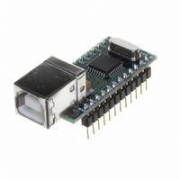
... DLP-USB245M-G USB to FIFO Parallel Interface Module The DLP-USB245M-G is the 2nd generation, lead free version of DLP Design’s USB adapter. This device adds extra functionality to it’s DLP-USB1 predecessor with a reduced component count and a new low price. DLP-USB245M FEATURES • Send / Receive Data over USB Bytes / sec • ...
Page 2
... By using FTDI’s virtual COM Port drivers, the peripheral looks like a standard COM Port to the application software. Commands to set the baud rate are ignored – the device always transfers data at its fastest rate regardless of the application’s baud rate setting. The latest versions of the drivers are available for download from DLP Design’s website at http://www.dlpdesign.com. ...
Page 3
... Unzip the file to a blank floppy disk or folder on your PC. The drivers can co-exist on the same floppy disk or folder since the INF files determine which set of drivers to load for each operating system version. Once loaded, the VCP drivers allow your application software, running on the host PC, to communicate with the DLP-USB245M as though it were connected to a COM (RS-232) port. ...
Page 4
... Download the serializer program from either dlpdesign.com or ftdichip.com. Unzip the package and place folder on the hard drive. 3. Select a power source for the DLP-USB245M module via pins 10, 11, and 12. Be sure to pull the RESET# pin high (pin 3). 4. Connect the DLP-USB245M board to the PC via a standard, 6-foot USB cable. This action initiates the loading of the USB drivers. When prompted, select the folder where the DLL version of the device drivers were stored Copyright © ...
Page 5
... EEPROM as well as the serial number and description strings stored in the EEPROM. At this point the DLP-USB245M is ready for use. Note that the DLP-USB245M will appear non-responsive if data sent from the host PC is not read from the FT245BM device by an attached microcontroller/microprocessor/DSP/FPGA/ etc… ...
Page 6
... Table 1 - DLP-USB245M PINOUT DESCRIPTION 1 12 Pin# Description 1 BOARD ID (Out) Identifies the board as either a DLP-USB245M or DLP-USB232M. High for DLP- USB232M and low for DLP-USB245M. 2 Ground 3 RESET# (In) Can be used by an external device to reset the FT245BM. If not required this pin must be tied to VCC. 4 RESETO# (Out) Output of the internal Reset Generator. Stays high impedance for ~ 2ms after VCC > ...
Page 7
... SND/WUP (In) If the DLP-USB245M is in USB suspend, a positive edge on this pin (WAKEUP) initiates a remote wakeup sequence. If the device is active (not in suspend) a positive edge on this pin (SEND) causes the data in the write buffer to be sent to the PC on the next USB Data-In request regardless of how many bytes are in the buffer ...
Page 8
... A Self Powered Device can take as much current as it likes during normal operation and USB suspend as it has its own Power Supply Self Powered Device can be used with any USB Host and both Bus and Self Powered USB Hubs. Copyright © DLP Design 2002 8 data WR ...
Page 9
... Figure 3 3.3V Figure 3 shows how to configure the DLP-USB245M to interface with a 3.3v logic device. In this example, the target electronics provides the 3.3 volts via the VCCIO line (pin 10) which in turn will cause the FIFO interface IO pins to drive out at 3.3v level. Bus Powered Circuit with Power Control USB Bus powered circuits need to be able to power down in USB suspend mode in order to meet the < ...
Page 10
... DLP-USB245M TIMING DIAGRAM – FIFO READ CYCLE RXF# RD# T3 D[7..0] D Description Min Max Unit Time Description T1 RD Active Pulse Width Pre-Charge Time T3 RD Active to Valid Data T4 Valid Data Hold Time from RD Inactive T5 RD Inactive to RXF# T6 RXF inactive after RD cycle DLP-USB1 TIMING DIAGRAM – FIFO WRITE CYCLE ...
Page 11
... Mechanical Drawings (PRELIMINARY) Inches(millimeters) unless otherwise noted 1.5 typ (38.1 typ) .235 typ (6.0 typ) .50 typ (12.7 typ) .16 typ (4.2 typ) Copyright © DLP Design 2002 DLP-USB245M User Manual .52 typ dia (13.2 typ) .19 typ dia (.46 typ) .6 typ (15.2 typ) .7 typ (17.8 typ) ...
Page 12
... Input Switching Threshold VHys Input Switching Hysteresis FIFO IO Pin Characteristics ( VCCIO = 3.3v ) Parameter Description Voh Output Voltage High Vol Output Voltage Low Vin Input Switching Threshold VHys Input Switching Hysteresis Copyright © DLP Design 2002 DLP-USB245M User Manual 150 Min Typ Max Units 4 ...
Page 13
... UCom Differential Common Mode UVDif Differential Input Sensitivity UDrvZ Driver Output Impedance Note 2 – Driver Output Impedance includes the external 27R series resistors on USBDP and USBDM pins. Copyright © DLP Design 2002 DLP-USB245M User Manual Min Typ Max Units 1.1 1.5 1 ...
Page 14
... This product and its documentation are supplied basis and no warranty as to their suitability for any particular purpose is either made or implied. DLP Design will not accept any claim for damages howsoever arising as a result of use or failure of this product. Your statutory rights are not affected. ...
Page 15
... Appendix A – DLP USB245M Schematic VCC-IO 13 VCC 26 VCC 3 AVCC 30 Copyright © DLP Design 2002 DLP-USB245M User Manual GND 17 GND 9 AGND 29 GND 5 Page ...