FDZ3N513ZT Fairchild Semiconductor, FDZ3N513ZT Datasheet
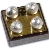
MOSFET N-CH 30V WLCSP 2X2

FDZ3N513ZT

Manufacturer Part Number
FDZ3N513ZT
Description
MOSFET N-CH 30V WLCSP 2X2
Manufacturer
Fairchild Semiconductor
Datasheet

Specifications of FDZ3N513ZT

Fet Type
MOSFET N-Channel, Schottky, Metal Oxide
Fet Feature
Logic Level Gate
Rds On (max) @ Id, Vgs
462 mOhm @ 300mA, 4.5V
Drain To Source Voltage (vdss)
30V
Current - Continuous Drain (id) @ 25° C
1.1A
Vgs(th) (max) @ Id
1.5V @ 250µA
Gate Charge (qg) @ Vgs
1nC @ 4.5V
Input Capacitance (ciss) @ Vds
85pF @ 15V
Power - Max
1W
Mounting Type
Surface Mount
Package / Case
*
Configuration
Dual
Transistor Polarity
N-Channel
Resistance Drain-source Rds (on)
462 mOhms
Forward Transconductance Gfs (max / Min)
0.5 S
Drain-source Breakdown Voltage
30 V
Gate-source Breakdown Voltage
5.5 V
Continuous Drain Current
1.1 A
Power Dissipation
1 W
Maximum Operating Temperature
+ 125 C
Mounting Style
SMD/SMT
Gate Charge Qg
1 nC
Minimum Operating Temperature
- 55 C
Lead Free Status / RoHS Status
Lead free / RoHS Compliant
Other names
FDZ3N513ZTTR
©2010 Fairchild Semiconductor Corporation
FDZ3N513ZT Rev. C
FDZ3N513ZT
Integrated NMOS and Schottky Diode
Features
Absolute Maximum Ratings
Thermal Characteristics
Package Marking and Ordering Information
V
V
P
I
V
I
T
ESD
R
R
D
O
Symbol
J
DS
GS
D
RRM
Monolithic NMOS and Schottky Diode
Ultra-small form factor 1mm x 1mm WLCSP
Max r
Max r
HBM ESD protection level > 2000V (Note3)
RoHS Compliant
θJA
θJA
WL-CSP 3D Bumps Facing Up View
, T
Part Number
FDZ3N513ZT
STG
DS(on)
DS(on)
S
NMOS Drain to Source Voltage
NMOS Gate to Source Voltage
Power Dissipation @ T
Maximum Continuous NMOS Drain Current
Schottky Repetitive Peak Reverse Voltage
Schottky Average Forward Current
Operating Junction and Storage Temperature
Electrostatic Discharge Protection
Thermal Resistance, Junction to Ambient - 1in
Thermal Resistance, Junction to Ambient - Minimum Pad
= 462 mΩ at V
= 520 mΩ at V
D
G
K
Device Marking
GS
GS
Pin 1
= 4.5 V, I
= 3.2 V, I
A
Z3
= 25°C
D
D
= 0.3 A
= 0.3 A
WL-CSP 3D Bumps Facing Down View
Parameter
WL-CSP 1.0X1.0
Package
2
, 2oz. Copper
1
General Description
The FDZ3N513ZT is a monolithic NMOS/ Schottky combination
(FETky) and is designed and wired to function as a discontinu-
ous conduction mode (DCM) boost LED power train for mobile
LED backlighting applications.
Application
Boost Converter Power Train for single cell Li-ion LED
backlighting
Reel Size
7”
(Note 1a)
(Note 1a)
(Note 1a)
(Note 1b)
WL-CSP 1.0X1.0 Bumps Facing Up View
CDM
Tape Width
8mm
Ratings
-0.3/5.5
-55/125
2000
100
260
1.1
0.3
30
25
1
www.fairchildsemi.com
5000 units
Quantity
July 2010
Units
°C/W
°C/W
°C
W
V
V
A
V
A
V

Related parts for FDZ3N513ZT

FDZ3N513ZT Summary of contents

Page 1

... Part Number Device Marking FDZ3N513ZT Z3 ©2010 Fairchild Semiconductor Corporation FDZ3N513ZT Rev. C General Description The FDZ3N513ZT is a monolithic NMOS/ Schottky combination (FETky) and is designed and wired to function as a discontinu- ous conduction mode (DCM) boost LED power train for mobile LED backlighting applications 0.3 A ...

Page 2

... Pulse Test: Pulse Width < 300μs, Duty cycle < 2.0%. 3. The diode connected between the gate and source serves only as protection ESD. No gate overvoltage rating is implied. ©2010 Fairchild Semiconductor Corporation FDZ3N513ZT Rev °C unless otherwise noted J Test Conditions = 250 μ ...

Page 3

... DUTY CYCLE = 0.5% MAX 1 150 C J 1.0 0.5 0 0.5 1 GATE TO SOURCE VOLTAGE (V) GS Figure 5. Transfer Characteristics ©2010 Fairchild Semiconductor Corporation FDZ3N513ZT Rev 25°C unless otherwise noted J 2.0 1.8 1.6 = 1.5 V 1.4 1.2 μ s 1.0 2.0 2.5 3.0 1600 1400 1200 1000 ...

Page 4

... Figure 9. Forward Bias Safe Operating Area - 125 REVERSE VOLTAGE (V) R Figure 11. Schottky Diode Reverse Current ©2010 Fairchild Semiconductor Corporation FDZ3N513ZT Rev 25°C unless otherwise noted J 500 100 0.9 1.2 0.0030 0.0025 1 ms 0.0020 10 ms 0.0015 100 ms 0.0010 0.0005 0.0000 -0.0005 10 100 ...

Page 5

... Figure 13. Single Pulse Maximum Power Dissipation 2 1 DUTY CYCLE-DESCENDING ORDER D = 0.5 0.2 0.1 0.05 0.1 0.02 0.01 0.01 0.001 - Figure 14. Junction-to-Ambient Transient Thermal Response Curve ©2010 Fairchild Semiconductor Corporation FDZ3N513ZT Rev 25°C unless otherwise noted PULSE WIDTH (s) SINGLE PULSE 260 C/W θ ...

Page 6

... Dimensional Outline and Pad Layout Product Specific Dimensions Product FDZ3N513ZTUCX ©2010 Fairchild Semiconductor Corporation FDZ3N513ZT Rev 1.000 +/-0.030 1.000 +/-0.030 0.018 0.018 www.fairchildsemi.com ...

Page 7

... Datasheet Identification Product Status Advance Information Formative / In Design Preliminary First Production No Identification Needed Full Production Obsolete Not In Production ©2010 Fairchild Semiconductor Corporation FDZ3N513ZT Rev. C Power-SPM™ ® ® PowerTrench SM PowerXS™ Programmable Active Droop™ ® QFET QS™ Quiet Series™ ...

Related keywords