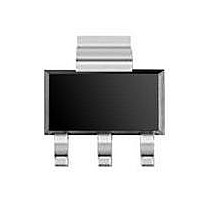
STN4NF20L STMicroelectronics, STN4NF20L Datasheet - Page 4

STN4NF20L
Manufacturer Part Number
STN4NF20L
Description
MOSFET N-CH 200V 1A SOT-223
Manufacturer
STMicroelectronics
Series
STripFET™r
Datasheet
1.STN4NF20L.pdf
(12 pages)
Specifications of STN4NF20L
Fet Type
MOSFET N-Channel, Metal Oxide
Fet Feature
Logic Level Gate
Rds On (max) @ Id, Vgs
1.5 Ohm @ 500mA, 10V
Drain To Source Voltage (vdss)
200V
Current - Continuous Drain (id) @ 25° C
1A
Vgs(th) (max) @ Id
3V @ 250µA
Gate Charge (qg) @ Vgs
0.9nC @ 10V
Input Capacitance (ciss) @ Vds
150pF @ 25V
Power - Max
3.3W
Mounting Type
Surface Mount
Package / Case
SOT-223 (3 leads + Tab), SC-73, TO-261
Configuration
Single
Transistor Polarity
N-Channel
Resistance Drain-source Rds (on)
1.5 Ohms
Drain-source Breakdown Voltage
200 V
Continuous Drain Current
1 A
Power Dissipation
3.3 W
Maximum Operating Temperature
+ 150 C
Mounting Style
SMD/SMT
Lead Free Status / RoHS Status
Lead free / RoHS Compliant
Other names
497-10779-2
Available stocks
Company
Part Number
Manufacturer
Quantity
Price
Company:
Part Number:
STN4NF20L
Manufacturer:
STM
Quantity:
718
Part Number:
STN4NF20L
Manufacturer:
ST
Quantity:
20 000
Electrical characteristics
2
4/12
Electrical characteristics
(Tcase = 25 °C unless otherwise specified)
Table 5.
Table 6.
Table 7.
Symbol
V
Symbol
Symbol
R
V
(BR)DSS
t
t
C
c(off)
I
I
C
DS(on)
C
GS(th)
Q
Q
d(v)
DSS
GSS
Q
R
t
t
oss
r
f
rss
iss
gs
gd
g
g
Voltage delay time
Voltage rise time
Current fall time
Crossing time
Input capacitance
Output capacitance
Reverse transfer
capacitance
Instrinsic gate
resistance
Total gate charge
Gate-source charge
Gate-drain charge
Drain-source
breakdown voltage
Zero gate voltage
drain current (V
Gate-body leakage
current (V
Gate threshold voltage V
Static drain-source on
resistance
On /off states
Dynamic
Switching times
Parameter
Parameter
Parameter
DS
= 0)
GS
= 0)
Doc ID 17445 Rev 2
V
R
(see
I
V
V
V
V
V
V
V
f=1 MHz open drain
V
V
(see
D
GS
GS
DD
GS
GS
GS
GS
DS
DD
G
DS
DS
= 1 mA, V
= 4.7 Ω, V
= Max rating
= Max rating, T
= 100 V, I
= ± 20 V, V
= V
= 10 V, I
= 5 V, I
= 25 V, f = 1 MHz,
= 0
= 10 V
= 160 V, I
Figure
Figure
Test conditions
Test conditions
Test conditions
DS
, I
D
12)
13)
GS
D
D
= 0.5 A
D
GS
D
= 250 µA
= 0.5 A
= 0
DS
= 0.5 A,
= 1 A,
= 10 V
=0
C
=125 °C
Min.
Min.
Min.
200
-
1
-
-
-
Typ.
10.4
15.4
Typ.
Typ.
1.13
150
3.6
5.5
0.9
2.6
6.9
1.1
30
2
4
2
STN4NF20L
± 100
Max.
Max
Max.
1.55
1.5
50
-
1
3
-
-
-
Unit
Unit
Unit
nC
nC
nC
ns
ns
ns
ns
µA
µA
nA
pF
pF
pF
Ω
V
V
Ω
Ω


