STMPE16M31PXQTR STMicroelectronics, STMPE16M31PXQTR Datasheet - Page 10
STMPE16M31PXQTR
Manufacturer Part Number
STMPE16M31PXQTR
Description
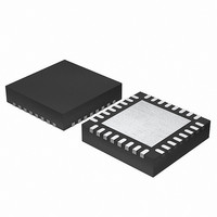
IC CTLR TOUCHKEY 16CHAN 32-QFN
Manufacturer
STMicroelectronics
Series
S-Touch™r
Type
Capacitive, PWM, Ratio Enginer
Specifications of STMPE16M31PXQTR
Featured Product
STMPE16M31PX
Number Of Inputs/keys
16 Key, Slider
Data Interface
I²C
Data Rate/sampling Rate (sps, Bps)
100k, 400k
Voltage Reference
External
Voltage - Supply
2.7 V ~ 5.5 V
Operating Temperature
-40°C ~ 85°C
Mounting Type
Surface Mount
Package / Case
32-VFQFN Exposed Pad
Supply Voltage
1.65 V to 1.95 V
Number Of Channels
16
Dimensions
4 mm L x 4 mm W x 0.8 mm H
Temperature Range
- 40 C to + 85 C
Termination Style
SMD/SMT
Lead Free Status / RoHS Status
Lead free / RoHS Compliant
Current - Supply
-
Resolution (bits)
-
Touch Panel Interface
-
Other names
497-10738-2
Available stocks
Company
Part Number
Manufacturer
Quantity
Price
Company:

Part Number:
STMPE16M31PXQTR
Manufacturer:
STM
Quantity:
12 495


I
10/75
2
C interface module
Acknowledge bit (ACK)
The acknowledge bit is used to indicate a successful byte transfer. The bus transmitter
releases the SDA after sending eight bits of data. During the ninth bit, the receiver pulls the
SDA low to acknowledge the receipt of the eight bits of data. The receiver may leave the
SDA in high state if it would to not acknowledge the receipt of the data.
Data input
The device samples the data input on SDA on the rising edge of the SCL. The SDA signal
must be stable during the rising edge of SCL and the SDA signal must change only when
SCL is driven low.
Memory addressing
For the bus master to communicate to the slave device, the bus master must initiate a Start
condition and be followed by the slave device address. Accompanying the slave device
address, there is a Read/W bit (R/W). The bit is set to 1 for Read and 0 for Write operation.
If a match occurs on the slave device address, the corresponding device gives an
acknowledgement on the SDA during the 9
from the bus by not responding to the transaction. The register memory map of the device is
8-bit address width. Therefore, the maximum number of register is 256 registers of 8-bit
width.
Table 6
Table 6.
Mode
Read
Write
illustrates the device operating modes that are supported.
Device operation modes
Bytes
≥1
≥1
START, Device Address, R/W
=0, Base register Address to be read
ReSTART, Device Address, R/W
=1, Data Read, STOP
If no STOP is issued, the Data Read can be continuously
preformed. The address is automatically incremented on
subsequent data read.
START, Device Address, R/W
=0, Register Address to be written, Data Write, STOP
If no STOP is issued, the Data Write can be continuously
performed. The address is automatically incremented on
subsequent write.
Doc ID 17058 Rev 2
th
bit time. If there is no match, it deselects itself
Initial sequence
STMPE16M31PX
Related parts for STMPE16M31PXQTR
Image
Part Number
Description
Manufacturer
Datasheet
Request
R

Part Number:
Description:
STMicroelectronics [RIPPLE-CARRY BINARY COUNTER/DIVIDERS]
Manufacturer:
STMicroelectronics
Datasheet:
Part Number:
Description:
STMicroelectronics [LIQUID-CRYSTAL DISPLAY DRIVERS]
Manufacturer:
STMicroelectronics
Datasheet:

Part Number:
Description:
BOARD EVAL FOR MEMS SENSORS
Manufacturer:
STMicroelectronics
Datasheet:
Part Number:
Description:
NPN TRANSISTOR POWER MODULE
Manufacturer:
STMicroelectronics
Datasheet:
Part Number:
Description:
TURBOSWITCH ULTRA-FAST HIGH VOLTAGE DIODE
Manufacturer:
STMicroelectronics
Datasheet:
Part Number:
Description:
Manufacturer:
STMicroelectronics
Datasheet:
Part Number:
Description:
DIODE / SCR MODULE
Manufacturer:
STMicroelectronics
Datasheet:
Part Number:
Description:
DIODE / SCR MODULE
Manufacturer:
STMicroelectronics
Datasheet:
Part Number:
Description:
Search -----> STE16N100
Manufacturer:
STMicroelectronics
Datasheet:
Part Number:
Description:
Search ---> STE53NA50
Manufacturer:
STMicroelectronics
Datasheet:
Part Number:
Description:
NPN Transistor Power Module
Manufacturer:
STMicroelectronics
Datasheet:
Part Number:
Description:
DIODE / SCR MODULE
Manufacturer:
STMicroelectronics
Datasheet: