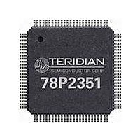
78P2351-IGT/F Maxim Integrated Products, 78P2351-IGT/F Datasheet - Page 14

78P2351-IGT/F
Manufacturer Part Number
78P2351-IGT/F
Description
LINE INTERFACE UNIT 100-LQFP
Manufacturer
Maxim Integrated Products
Specifications of 78P2351-IGT/F
Number Of Channels Per Chip
1
Propagation Delay Time
10 ns
Supply Voltage (max)
3.45 V
Supply Voltage (min)
3.15 V
Maximum Operating Temperature
+ 85 C
Package / Case
LQFP-100
Minimum Operating Temperature
- 40 C
Mounting Style
SMD/SMT
Lead Free Status / RoHS Status
Lead free / RoHS Compliant
Available stocks
Company
Part Number
Manufacturer
Quantity
Price
Company:
Part Number:
78P2351-IGT/F
Manufacturer:
VISHAY
Quantity:
14 105
Company:
Part Number:
78P2351-IGT/F
Manufacturer:
MAXIM
Quantity:
4
Company:
Part Number:
78P2351-IGT/F
Manufacturer:
Maxim Integrated
Quantity:
10 000
Design Guidelines for TERIDIAN 78P235x LIUs
Eye Diagram
The Eye Diagram provides a longer-term view of the signal, taking into account the relative time position of
successive pulses. It provides less information about pulse shape but allows a more thorough analysis of the
cumulative effects of wander and jitter. Eye diagrams require the use of DPO mode or other long-term persistence
method to preserve information from the preceding pulses then overlaying them in a continuous fashion. The
timing and pulse width variations are then displayed as a widening of the eye diagram’s traces, which must
remain within the template to meet specification.
A few words about transmit timing modes in the 78P235x
The 78P235x LIUs use delay lock loop (DLL) technology to track the incoming data and recovery timing. In the
78P235x, there are two different modes in which the integrated CDR is used to recovery the transmit clock. This
section will describe both and their effects on CMI pulse mask testing.
Most transmit timing modes of the 78P235x are synchronous (re-timing) modes where a system reference
clock is provided to the LIU that is source synchronous with the timing of the transmit data source (i.e. SDH
Overhead Processor), E4 Mapper). In this mode of operation, the transmit output is re-timed to eliminate any jitter
caused by clock recovery or serialization.
For application where only data is available at the system (NRZ) interface, a plesiochronous transmit timing
mode is available. In this mode, the recovered transmit clock is used for CMI encoding and pulse shaping.
Page 14 of 15
“Maximum Eye Diagram” @ 0ft
+/- 70ppm or better
System Reference
+/- 20ppm for STM1
+/- 15ppm for E4
Tx Data In
XO
Tx Data In
235x Transmit - Synchronous (re-timing) modes
BW ~ 1 MHz
BW ~ 1 MHz
PLL / VCO
PLL / VCO
2008 Teridian Semiconductor Corp.
622 MHz
622 MHz
235x Transmit - Plesiochronous mode
De-coupled Tx output exhibits lower phase
jitter due to re-timing with FIFO
and
BW = 80 kHz
32 phase taps (100ps )
Direct coupled Tx output will exhibit
high freq. phase jitter
Div/2
Div/2
“Small Eye Diagram” @ 225ft
DLL
DLL
D
CK
FIFO
TX DATA OUT
TX DATA OUT
Rev 2.1


