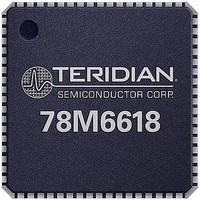
78M6618-IM/F Maxim Integrated Products, 78M6618-IM/F Datasheet - Page 27

78M6618-IM/F
Manufacturer Part Number
78M6618-IM/F
Description
IC PWR MEASUREMENT OCTAL 68-QFN
Manufacturer
Maxim Integrated Products
Type
Octal Power and Energy Measurement ICr
Datasheet
1.78M6618-IMF.pdf
(32 pages)
Specifications of 78M6618-IM/F
Core
80515
Core Architecture
80515
Data Bus Width
8 bit
Data Ram Size
4 KB
Interface Type
SPI, UART
Maximum Clock Frequency
500 KHz
Maximum Operating Temperature
+ 85 C
Minimum Operating Temperature
- 40 C
Mounting Style
SMD/SMT
Number Of Programmable I/os
19
Number Of Timers
1
On-chip Adc
21 bit, 10 Channel
Operating Supply Voltage
3.3 V
Package / Case
QFN-68
Processor Series
78M6618
Program Memory Size
128 KB
Program Memory Type
Flash
Lead Free Status / RoHS Status
Lead free / RoHS Compliant
Available stocks
Company
Part Number
Manufacturer
Quantity
Price
Company:
Part Number:
78M6618-IM/F
Manufacturer:
ATMEL
Quantity:
240
DS_6618_005
4.1
4.2
1)
The circuit number denotes the equivalent circuit, as specified under
Rev. 1.4
4 Pin Descriptions
Name
GNDA
GNDD
V3P3A
V3P3SYS
V3P3D
VBAT
V2P5
Name
IA, IB,
IC, ID,
IE, IF,
IG, IH
VA, VB
V1
VREF
XIN
XOUT
Pin types: P = Power, O = Output, I = Input, I/O = Input/Output
Power and Ground Pins
Analog Pins
Type
O
I
I
I
I
Type
O
O
P
P
P
P
P
Circuit
Circuit
6
6
7
9
8
13
12
10
–
–
–
–
Line Current Sense Inputs: These pins are voltage inputs to the internal A/D
converter. Typically, they are connected to the outputs of current sensors.
Unused pins must be tied to V3P3A.
Line Voltage Sense Inputs: These pins are voltage inputs to the internal A/D
converter. Typically, they are connected to the outputs of resistor dividers.
Unused pins must be tied to V3P3A.
Comparator Input: This pin is a voltage input to the internal comparator.
The voltage applied to the pin is compared to the internal BIAS voltage
(1.6 V). If the input voltage is above VBIAS, the comparator output will be
high (1). If the comparator output is low, a voltage fault will occur. A series
5 kΩ resistor should be connected from V1 to the resistor divider.
Voltage Reference for the ADC. Normally disabled and left unconnected. If
enabled, a 0.1 µF capacitor to V3P3A should be connected to this pin.
Crystal Inputs: A 32 kHz crystal should be connected across these pins.
Typically, a 33 pF capacitor is also connected from XIN to GNDA and a
15 pF capacitor is connected from XOUT to GNDA. It is important to mi-
nimize the capacitance between these pins. See the crystal manufacturer
datasheet for details. If an external clock is used, a 150 mV (p-p) clock
signal should be applied to XIN, and XOUT should be left unconnected.
Analog ground: This pin should be connected directly to the ground
plane.
Digital ground: This pin should be connected directly to the ground plane.
Analog power supply: A 3.3 V power supply should be connected to this
pin, must be the same voltage as V3P3SYS.
System 3.3 V supply. This pin should be connected to a 3.3 V power
supply.
Auxiliary voltage output of the chip, controlled by the internal 3.3 V
selection switch. In mission mode, this pin is internally connected to
V3P3SYS. In BROWNOUT mode, it is internally connected to VBAT.
This pin is left unconnected in LCD and sleep mode. A bypass capacitor
to ground should not exceed 0.1 µF.
Battery backup and oscillator power supply. A battery or super-capacitor
is to be connected between VBAT and GNDD. If no battery is used,
connect VBAT to V3P3SYS.
Output of the internal 2.5 V regulator. Leave this pin open.
Table 26: Power and Ground Pins
Table 27: Analog Pins
Description
Description
Section
5,
I/O Equivalent
78M6618 Data Sheet
Circuits.
27


